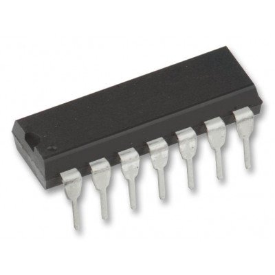
CD4023 Triple 3-Input NAND Gate IC DIP-14 Package
CD4023 NAND gate provide the system designer with direct implementation of the NAND function and supplement the existing family of CMOS gates. All inputs and outputs are buffered.
Apple Shopping Event
Hurry and get discounts on all Apple devices up to 20%
Sale_coupon_15
₹42.48
Inclusive of GST
- Pick up from the Robotwala Store
To pick up today
Free
- Shiprocket from Air
Our courier will deliver to the specified address
3-4 Days
139
- Shiprocket from Surface
courier will deliver to the specified address
5-7 Days
90
- Warranty 1 year
- Free 30-Day returns
Payment Methods:
Description
CD4023 NAND gate provide the system designer with direct implementation of the NAND function and supplement the existing family of CMOS gates. All inputs and outputs are buffered.
The CD4023 type is supplied in 14-lead hermetic dual-in-line ceramic packages (F3A suffix), 14-lead dual-in-line plastic packages (E suffix), 14-lead small-outline packages (M, MT, M96, and NSR suffixes), and 14-lead thin shrink small-outline packages (PWR suffix). The CD4023 type is also supplied in 14-lead thin shrink small-outline packages (PW suffix).
Features:-
- Propagation delay time = 60 ns (typ.) at CL = 50 pF, VDD = 10 V
- Buffered inputs and outputs
- Standardized symmetrical output characteristics
- Maximum input current of 1 ?A at 18 V over-full package temperature range; 100 nA at 18 V and 25?C
- 100% tested for quiescent current at 20 V
- 5-V, 10-V, and 15-V parametric ratings
- Noise margin (over full package temperature range:
1 V at VDD = 5 V
2 V at VDD = 10 V
2.5 at VDD = 15 V - Meets all requirements of JEDEC Tentative Standard No. 13B, “Standard Specifications for Description of “B” Series CMOS Devices”.
Specifications:-
| Parameter | Specification |
| Part number | CD4023B |
| Technology Family | CD4000 |
| VCC (Min) (V) | 3 |
| VCC (Max) (V) | 18 |
| Channels (#) | 4 |
| Inputs per channel | 2 |
| IOL (Max) (mA) | 1.5 |
| IOH (Max) (mA) | -1.5 |
| Input type | Standard CMOS |
| Output type | Push-Pull |
| Features | Standard Speed (tpd > 50ns) |
| Rating | See Data Sheet |
| Data rate (Max) (Mbps) | 8 |
| Operating temperature range (C) | -55 to 125 |
| Package size: mm2:W x L (PKG) | 14PDIP: 181 mm2: 9.4 x 19.3 (PDIP|14) |
| Package Group | PDIP|14 |
Related Document:-
Additional information
Operating voltage | 2.5 3.0V |
Pixel Resolution | 0.3MP |
Photosensitive array | 640 x 480 |
Optical Size | 1.6 inch |
Angel of view | 67 degrees |
Maximum Frame Rate | 30fps VGA |
Sensitivity | 1.3V/(Lux-sec) |
Dormancy | Less than 20A |
Power consumption | 60mW/15fpsVGA YUV |
Temperature operation Range | -30 C ~ 70 C |
Pixel area | 3.6 x 3.6 m |
Signal to noise ratio (SNR) | 46 dB |
Dynamic range | 52 dB |






 Boards & Modules
 ARM Microcontroller
 AVR Microcontroller Board
 Arduino boards
 Advance Development Boards
 8051 Development Board

 Audio Amplifier Module
 Current & Volatage Sensor
 Breakout Board
 Flame Sensors
 Force Sensor
 Gas Sensors
 Hall Effect Sensor
 Humidity & Temperature Sensor
 LED Module
 PIR Sensor
 Pressure Sensors
 Proximity Sensor
 Relay Module
 Real Time Clock (RTC) Module
 Touch Sensor
 Ultrasonic Sensor
 Water Level & Water Flow Sensor
 Weighing Scale Sensor


 Ai Thinker ESp Wifi Module
 Pic Devlopment Board & programmer
 Led lights & Strips
 PCBs & Breadboard
 Potentiometer
 Power Transistors
 Resistor & Smd & inductor
 Switches
 Aluminium Heat Sink
 Buzzer & Speaker
 capacitor
 Crystal Oscillators
 Doides
 Electric Fuses
 ICs & Dips
 Power supply module
 Transformer
 Relay Module
 Kits
Kits Magnet
 RF Connectors
 PCT and DC Connectors
 Wires & Heat Shrink
 FFC, FPC, Berg connectors
 Nextion
 Segment
 Seedstudio
 Waveshare
 E Bike Batteries
 E bike Battery Case
 E bike Connectors
 E bike Display
 E bike Kit
 E bike Motors & Controllers
 Electronics Accessories
 Mechanical Accessories
 Display
 Cameras
Reviews
There are no reviews yet.