


Related Products
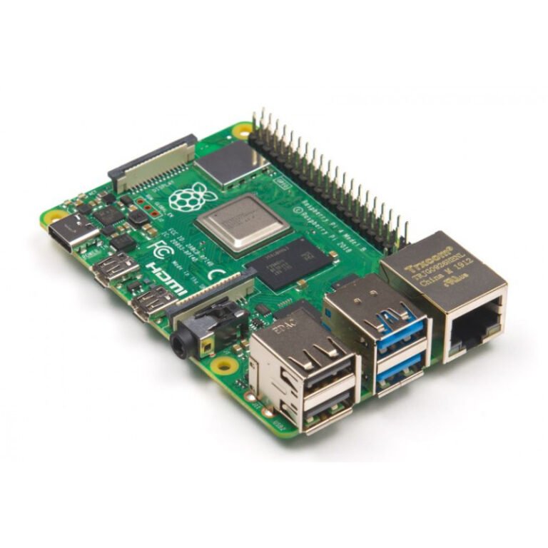
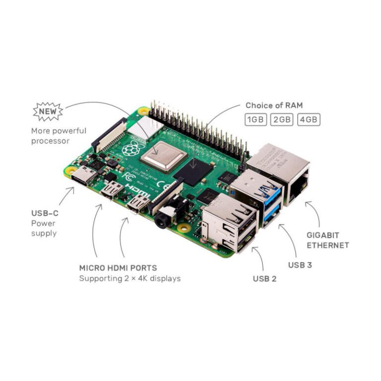
Raspberry Pi 4 Model B with 4GB Ram (Latest & Original)
Finally what we all are waiting for, Raspberry Pi Foundation has launched their Latest and original Raspberry Pi 4 Model B in 3 versions:-
1. Raspberry Pi 4 Model B with 1 GB Ram
2. Raspberry Pi 4 Model B with 2 GB Ram
3. Raspberry Pi 4 Model B with 4 GB Ram
Buy Raspberry Pi 4 Model B with 4 GB Ram Starter Kit with all necessary accessories at Low Price.
You can also buy Raspberry Pi 4 Model B with 1 GB Ram Starter Kit and
Raspberry Pi 4 Model B with 2 GB Ram Starter Kit at best price in India.
0-24 24V 2A Step Down Transformer
0-24 2Amp Step Down Transformer is a general purpose chassis mounting mains transformer. Transformer has 230V primary winding and non-center tapped secondary winding. The transformer has flying colored insulated connecting leads ( Approx 100 mm long ). The Transformer act as step down transformer reducing AC - 230V to AC - 24V.


 Boards & Modules
 ARM Microcontroller
 AVR Microcontroller Board
 Arduino boards
 Advance Development Boards
 8051 Development Board
 Audio Amplifier Module
 Current & Volatage Sensor
 Breakout Board
 Flame Sensors
 Force Sensor
 Gas Sensors
 Hall Effect Sensor
 Humidity & Temperature Sensor
 LED Module
 PIR Sensor
 Pressure Sensors
 Proximity Sensor
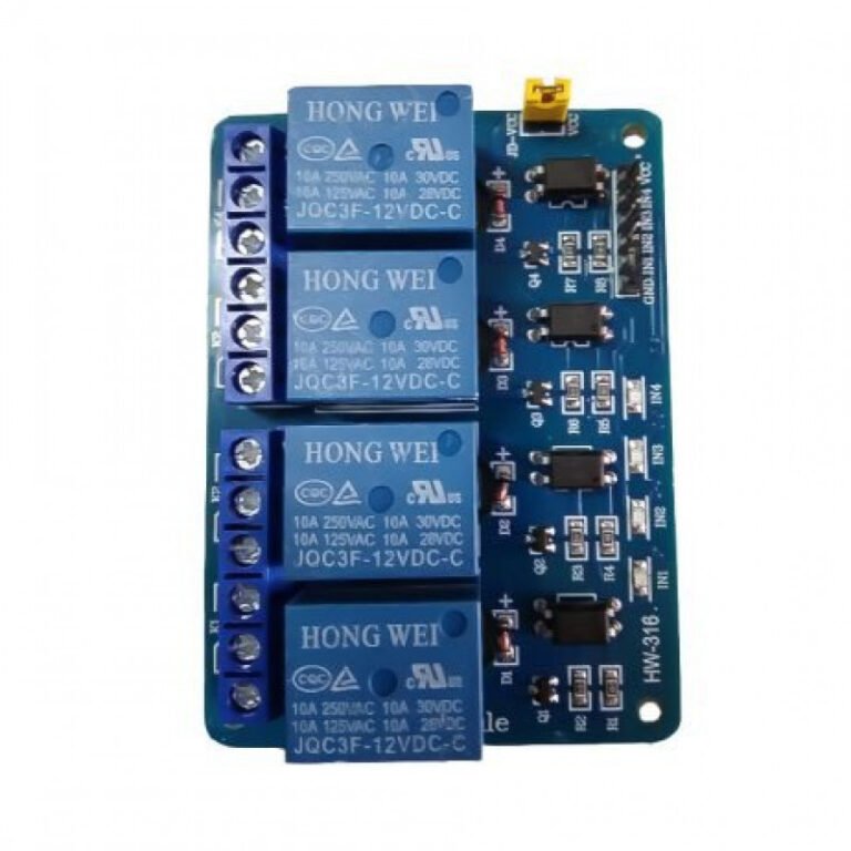
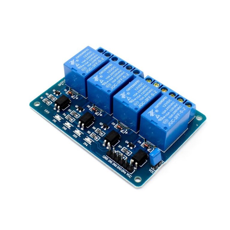
 Relay Module
 Real Time Clock (RTC) Module
 Touch Sensor
 Ultrasonic Sensor
 Water Level & Water Flow Sensor
 Weighing Scale Sensor


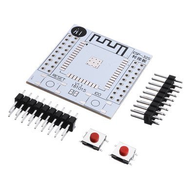
 Ai Thinker ESp Wifi Module
 Pic Devlopment Board & programmer
 Led lights & Strips
 PCBs & Breadboard
 Potentiometer
 Power Transistors
 Resistor & Smd & inductor
 Switches
 Aluminium Heat Sink
 Buzzer & Speaker
 capacitor
 Crystal Oscillators
 Doides
 Electric Fuses
 ICs & Dips
 Power supply module
 Transformer
 Relay Module
 Kits
Kits Magnet
 RF Connectors
 PCT and DC Connectors
 Wires & Heat Shrink
 FFC, FPC, Berg connectors
 Nextion
 Segment
 Seedstudio
 Waveshare
 E Bike Batteries
 E bike Battery Case
 E bike Connectors
 E bike Display
 E bike Kit
 E bike Motors & Controllers
 Electronics Accessories
 Mechanical Accessories
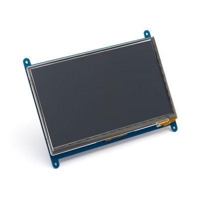
 Display
 Cameras
Reviews
There are no reviews yet.