

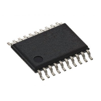
74HC30 IC ? (SMD Package) – 8-input NAND Gate IC (7430 IC)
74HC32 IC – (SMD Package) – Quad 2-Input OR Gate IC (7432 IC)
The 74HC32 is a 14 Pin Quad 2-Input OR Gate SMD IC. The 74HC32 provides four independent 2-input OR gates with standard push-pull outputs. The device is designed for operation with a power supply range of 2.0V to 6.0V. Inputs include clamp diodes. This enables the use of current limiting resistors to interface inputs to voltages in excess of VCC.
74HC32 Quad 2-Input OR Gate IC (7432 IC) DIP-14 Package
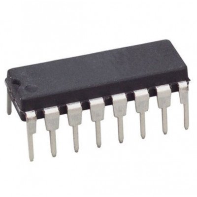
74HC366 Hex Inverting Buffer Line Driver IC (74366 IC) DIP-16 Package
The 74HC366; 74HCT366 is a hex inverting buffer/line driver with 3-state outputs controlled by the output enable inputs (OEn). A HIGH on OEn causes the outputs to assume a high impedance OFF-state. Inputs include clamp diodes. This enables the use of current limiting resistors to interface inputs to voltages in excess of VCC

74HC368 IC – (SMD Package) – Hex Inverting Buffer Line Driver IC (74368 IC)
The 74HC368; 74HCT368 is a hex inverting buffer/line driver with 3-state outputs controlled by the output enable inputs (nOE). A HIGH on nOE causes the outputs to assume a high impedance OFF-state. Inputs include clamp diodes enable the use of current limiting resistors to interface inputs to voltages in excess of VCC.
74HC373 IC – (SMD Package) – Octal D-Type Latch 3-State Outputs IC (74373 IC)
The 74HC373 high speed octal D-type latches utilize advanced silicon-gate CMOS technology. They possess the high noise immunity and low power consumption of standard CMOS integrated circuits, as well as the ability to drive 15 LS-TTL loads. Due to the large output drive capability and the 3-STATE feature, these devices are ideally suited for interfacing with bus lines in a bus organized system. When the LATCH ENABLE input is HIGH, the Q outputs will follow the D inputs. When the LATCH ENABLE goes LOW, data at the D inputs will be retained at the outputs until LATCH ENABLE returns HIGH again. When a high logic level is applied to the OUTPUT CONTROL input, all outputs go to a high impedance state, regardless of what signals are present at the other inputs and the state of the storage elements. The 74HC logic family is speed, function, and pin-out compatible with the standard 74LS logic family. All inputs are protected from damage due to static discharge by internal diode clamps to VCC and ground.
74HC373 Octal D-Type Latch 3-State Output IC (74373 IC) DIP-20 Package
The 74HC373 high speed octal D-type latches utilize advanced silicon-gate CMOS technology. They possess the high noise immunity and low power consumption of standard CMOS integrated circuits, as well as the ability to drive 15 LS-TTL loads. Due to the large output drive capability and the 3-STATE feature, these devices are ideally suited for interfacing with bus lines in a bus organized system.

74HC374 3-State Output Octal D-Type Flip-Flop IC (74374 IC) DIP-20 Package
74HC374 is a 20 Pin 3-State output Octal D-Type Flip-Flop IC having 2V to 6V Operating Voltage range with 7.8mA output current and high noise immunity. It has the ability to drive 15 LS-TTL loads. Due to the large output drive capability and the 3-STATE feature, these devices are ideally suited for interfacing with bus lines in a bus organized system. The eight edge-triggered flip-flops enter data into

74HC374 IC – (SMD Package) – 3-State Output Octal D-Type Flip-Flop IC (74374 IC)
The 74HC374 high speed Octal D-Type Flip-Flops utilize advanced silicon-gate CMOS technology. They possess the high noise immunity and low power consumption of standard CMOS integrated circuits, as well as the ability to drive 15 LS-TTL loads. Due to the large output drive capability and the 3-STATE feature, these devices are ideally suited for interfacing with bus lines in a bus organized system. These devices are positive edge triggered flip-flops. Data at the D inputs, meeting the setup and hold time requirements, are transferred to the Q outputs on positive going transitions of the CLOCK (CK) input. When a high logic level is applied to the OUTPUT CONTROL (OC) input, all outputs go to a high impedance state, regardless of what signals are present at the other inputs and the state of the storage elements. The 74HC logic family is speed, function, and pinout compatible with the standard 74LS logic family. All inputs are protected from damage due to static discharge by internal diode clamps to VCC and ground.
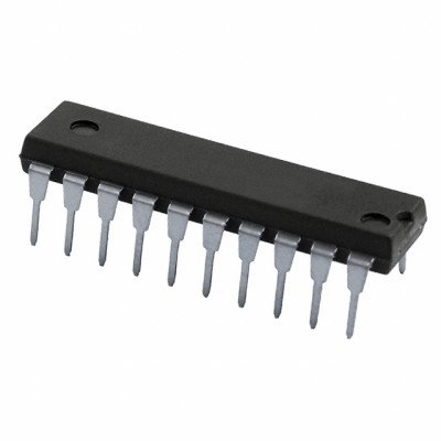
74HC390 Dual 4-bit Decade Ripple Counter IC (74390 IC) DIP-16 Package

74HC390 IC – (SMD Package) – Dual 4-bit Decade Ripple Counter IC (74390 IC)
The 74HC390 is a dual 4-bit decade ripple counter divided into four separately clocked sections. The counters have two divide-by-2 sections and two divide-by-5 sections. These sections share an asynchronous master reset input (nMR) and can be used in a BCD decade or bi-quinary configuration. If master reset inputs 1MR and 2MR are used to clear all 8 bits of the counter simultaneously, numerous counting configurations are possible within one package. Section clocks nCP0 and nCP1, allow ripple counter or frequency division applications of divide-by-2, 4, 5, 10, 20, 25, 50 or 100. The HIGH-to-LOW transition of the clock inputs nCP0 and nCP1 trigger each section. For BCD decade operation, the nQ0 output is connected to the nCP1 input of the divide-by-5 section. For bi-quinary decade operation, the nQ3 output is connected to the nCP0 input and nQ0 becomes the decade output. A HIGH on the nMR input overrides the clocks and sets the four outputs LOW. Inputs include clamp diodes. It enables the use of current limiting resistors to interface inputs to voltages in excess of VCC.

 Boards & Modules
 ARM Microcontroller
 AVR Microcontroller Board
 Arduino boards
 Advance Development Boards
 8051 Development Board
 Audio Amplifier Module
 Current & Volatage Sensor
 Breakout Board
 Flame Sensors
 Force Sensor
 Gas Sensors
 Hall Effect Sensor
 Humidity & Temperature Sensor
 LED Module
 PIR Sensor
 Pressure Sensors
 Proximity Sensor
 Relay Module
 Real Time Clock (RTC) Module
 Touch Sensor
 Ultrasonic Sensor
 Water Level & Water Flow Sensor
 Weighing Scale Sensor


 Ai Thinker ESp Wifi Module
 Pic Devlopment Board & programmer
 Led lights & Strips
 PCBs & Breadboard
 Potentiometer
 Power Transistors
 Resistor & Smd & inductor
 Switches
 Aluminium Heat Sink
 Buzzer & Speaker
 capacitor
 Crystal Oscillators
 Doides
 Electric Fuses
 ICs & Dips
 Power supply module
 Transformer
 Relay Module
 Kits
Kits Magnet
 RF Connectors
 PCT and DC Connectors
 Wires & Heat Shrink
 FFC, FPC, Berg connectors
 Nextion
 Segment
 Seedstudio
 Waveshare
 E Bike Batteries
 E bike Battery Case
 E bike Connectors
 E bike Display
 E bike Kit
 E bike Motors & Controllers
 Electronics Accessories
 Mechanical Accessories
 Display
 Cameras