

74LS151 IC – (SMD Package) 8-Input Digital Multiplexer IC (74151 IC)
This data selector/multiplexer contains full on-chip decoding to select the desired data source. The 74LS151 selects one-of-eight data sources. The 74LS151 has a strobe input which must be at a low logic level to enable these devices. A high level at the strobe forces the W output HIGH, and the Y output LOW. The 74LS151 features complementary W and Y outputs.
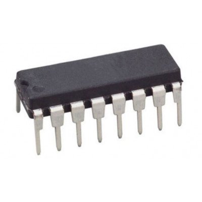
74LS153 Dual 1-of-4 Line Data Selector/Multiplexer IC (74153 IC) DIP-16 Package

74LS153 IC – (SMD Package) – Dual 1-of-4 Line Data Selectors/Multiplexers IC (74153 IC)
The 74LS153 is a very high speed Dual 4-Input Multiplexer with common select inputs and individual enable inputs for each section. It can select two bits of data from four sources. The two buffered outputs present data in the true (non-inverted) form. In addition to multiplexer operation, the LS153 can generate any two functions of three variables. The LS153 is fabricated with the Schottky barrier diode process for high speed and is completely compatible with all Motorola TTL families. The following are the features:-
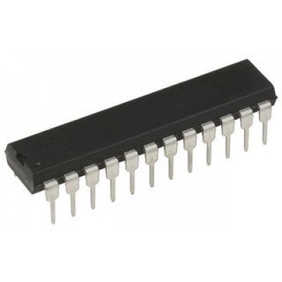
74LS154 4-Line to 16-Line Decoder/Demultiplexer IC (74154 IC) DIP-24 Package
In 74LS154 IC, Each of these 4-line-to-16-line decoders utilizes TTL circuitry to decode four binary-coded inputs into one of sixteen mutually exclusive outputs when both the strobe inputs, G1 and G2, are LOW. The demultiplexing function is performed by using the 4 input lines to address the output line, passing data from one of the strobe inputs with the other strobe input LOW. When either strobe input is HIGH, all outputs are HIGH. These demultiplexers are ideally suited for implementing high-performance memory decoders. All inputs are buffered and input clamping diodes are provided to minimize transmission-line effects and thereby simplify system design.

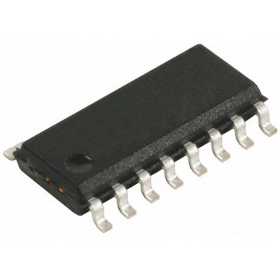
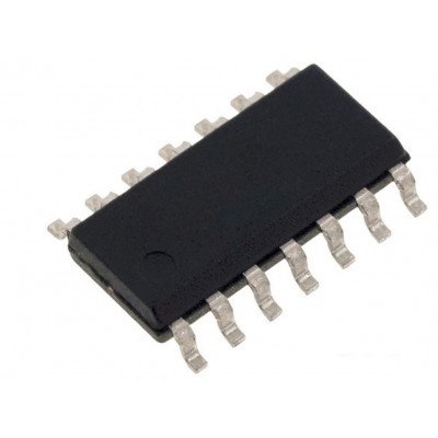
74LS158 IC – (SMD Package) Quad 2-Input Multiplexer IC (74158 IC)
The 74LS158 is a high speed Quad 2-input Multiplexer. It selects four bits of data from two sources using the common Select and Enable inputs. The four buffered outputs present the selected data in the inverted form. The LS158 can also generate any four of the 16 different functions of two variables. The LS158 is fabricated with the Schottky barrier diode process for high speed and is completely compatible with all Motorola TTL families
74LS158 Quad 2 -Input Multiplexer IC (74158) DIP-16 Package
The 74LS158 is a high speed Quad 2-input Multiplexer. It selects four bits of data from two sources using the common Select and Enable inputs. The four buffered outputs present the selected data in the inverted form. The LS158 can also generate any four of the 16 different functions of two variables. The LS158 is fabricated with the Schottky barrier diode process for high speed and is completely compatible with all Motorola TTL families
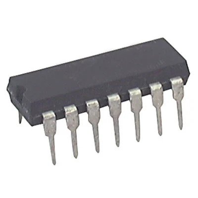
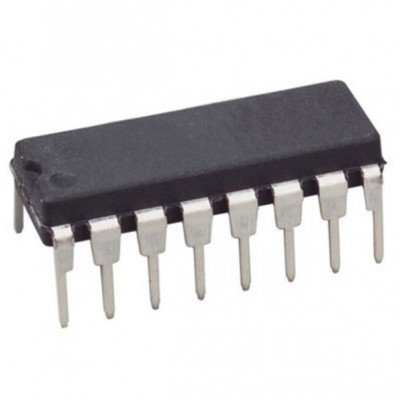
74LS161 4-Bit Synchronous Binary Counter IC (74161) DIP-14 Package
74LS161 4-Bit Binary Counter IC circuit designed as a synchronous reversible up-down counter. These synchronous, presettable counters provide an internal carry look-ahead feature for application in high-speed counting designs. The carry output decoded via a NOR gate. Thus preventing spikes during the normal counting mode of operation 74LS161 comes with a 4-bit binary counter in which Synchronous operation provided by all flip-flops clocked simultaneously. As a result, the outputs change simultaneously as instructed by the count-enable inputs and internal gating. This mode of operation eliminates the output counting spikes normally associated with asynchronous (ripple clock) counters. A buffered clock input triggers the four flip-flops on the rising (positive-going) fringe of the clock input waveform.
74LS161 IC – (SMD Package) 4-Bit Synchronous Binary Counter IC (74161 IC)
74LS161 4-Bit Binary Counter IC circuit designed as a synchronous reversible up-down counter. These synchronous, presettable counters provide an internal carry look-ahead feature for application in high-speed counting designs. The carry output decoded via a NOR gate. Thus preventing spikes during the normal counting mode of operation 74LS161 comes with a 4-bit binary counter in which Synchronous operation provided by all flip-flops clocked simultaneously. As a result, the outputs change simultaneously as instructed by the count-enable inputs and internal gating. This mode of operation eliminates the output counting spikes normally associated with asynchronous (ripple clock) counters. A buffered clock input triggers the four flip-flops on the rising (positive-going) fringe of the clock input waveform.

74LS166 8-Bit Shift Register Digital IC (74166) DIP-16 Package
The 74LS166 is an 8-Bit Shift Register. Designed with all inputs buffered, the drive requirements are lowered to one 74LS standard load. By utilizing input clamping diodes, switching transients are minimized and system design simplified. The LS166 is a parallel-in or serial-in, serial-out shift register and has a complexity of 77 equivalent gates with gated clock inputs and an overriding clear input. The shift/load input establishes the parallel-in or serial-in mode. When high, this input enables the serial data input and couples the eight flip-flops for serial shifting with each clock pulse. Synchronous loading occurs on the next clock pulse when this is low and the parallel data inputs are enabled. Serial data flow is inhibited during parallel loading. Clocking is done on the low-to-high level edge of the clock pulse via a two input positive NOR gate, which permits one input to be used as a clock enable or clock inhibit function. Clocking is inhibited when either of the clock inputs are held high, holding either input low enables the other clock input. This will allow the system clock to be free running and the register stopped on command with the other clock input. A change from low-to-high on the clock inhibit input should only be done when the clock input is high. A buffered direct clear input overrides all other inputs, including the clock, and sets all flip-flops to zero.

74LS166 IC – (SMD Package) 8-Bit Shift Register Digital IC (74166 IC)
The 74LS166 is an 8-Bit Shift Register. Designed with all inputs buffered, the drive requirements are lowered to one 74LS standard load. By utilizing input clamping diodes, switching transients are minimized and system design simplified. The LS166 is a parallel-in or serial-in, serial-out shift register and has a complexity of 77 equivalent gates with gated clock inputs and an overriding clear input. The shift/load input establishes the parallel-in or serial-in mode. When high, this input enables the serial data input and couples the eight flip-flops for serial shifting with each clock pulse. Synchronous loading occurs on the next clock pulse when this is low and the parallel data inputs are enabled. Serial data flow is inhibited during parallel loading. Clocking is done on the low-to-high level edge of the clock pulse via a two input positive NOR gate, which permits one input to be used as a clock enable or clock inhibit function. Clocking is inhibited when either of the clock inputs are held high, holding either input low enables the other clock input. This will allow the system clock to be free running and the register stopped on command with the other clock input. A change from low-to-high on the clock inhibit input should only be done when the clock input is high. A buffered direct clear input overrides all other inputs, including the clock, and sets all flip-flops to zero.

74LS170 IC – (SMD Package) Low-power 4×4 Register IC (74170 IC)
The 74LS170 is a high-speed, low-power 4 x 4 Register File organized as four words by four bits. Separate read and write inputs, both address and enable, allow simultaneous read and write operation. Open-collector outputs make it possible to connect up to 128 outputs in a wired-AND configuration to increase the word capacity up to 512 words. Any number of these devices can be operated in parallel to generate an n-bit length. The 74LS670 provides a similar function to this device but it features 3-state outputs

 Boards & Modules
 ARM Microcontroller
 AVR Microcontroller Board
 Arduino boards
 Advance Development Boards
 8051 Development Board
 Audio Amplifier Module
 Current & Volatage Sensor
 Breakout Board
 Flame Sensors
 Force Sensor
 Gas Sensors
 Hall Effect Sensor
 Humidity & Temperature Sensor
 LED Module
 PIR Sensor
 Pressure Sensors
 Proximity Sensor
 Relay Module
 Real Time Clock (RTC) Module
 Touch Sensor
 Ultrasonic Sensor
 Water Level & Water Flow Sensor
 Weighing Scale Sensor


 Ai Thinker ESp Wifi Module
 Pic Devlopment Board & programmer
 Led lights & Strips
 PCBs & Breadboard
 Potentiometer
 Power Transistors
 Resistor & Smd & inductor
 Switches
 Aluminium Heat Sink
 Buzzer & Speaker
 capacitor
 Crystal Oscillators
 Doides
 Electric Fuses
 ICs & Dips
 Power supply module
 Transformer
 Relay Module
 Kits
Kits Magnet
 RF Connectors
 PCT and DC Connectors
 Wires & Heat Shrink
 FFC, FPC, Berg connectors
 Nextion
 Segment
 Seedstudio
 Waveshare
 E Bike Batteries
 E bike Battery Case
 E bike Connectors
 E bike Display
 E bike Kit
 E bike Motors & Controllers
 Electronics Accessories
 Mechanical Accessories
 Display
 Cameras