


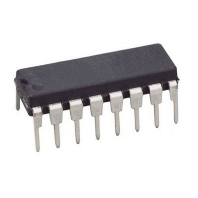
74LS166 8-Bit Shift Register Digital IC (74166) DIP-16 Package
The 74LS166 is an 8-Bit Shift Register. Designed with all inputs buffered, the drive requirements are lowered to one 74LS standard load. By utilizing input clamping diodes, switching transients are minimized and system design simplified. The LS166 is a parallel-in or serial-in, serial-out shift register and has a complexity of 77 equivalent gates with gated clock inputs and an overriding clear input. The shift/load input establishes the parallel-in or serial-in mode. When high, this input enables the serial data input and couples the eight flip-flops for serial shifting with each clock pulse. Synchronous loading occurs on the next clock pulse when this is low and the parallel data inputs are enabled. Serial data flow is inhibited during parallel loading. Clocking is done on the low-to-high level edge of the clock pulse via a two input positive NOR gate, which permits one input to be used as a clock enable or clock inhibit function. Clocking is inhibited when either of the clock inputs are held high, holding either input low enables the other clock input. This will allow the system clock to be free running and the register stopped on command with the other clock input. A change from low-to-high on the clock inhibit input should only be done when the clock input is high. A buffered direct clear input overrides all other inputs, including the clock, and sets all flip-flops to zero.

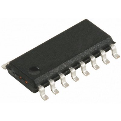
74LS166 IC – (SMD Package) 8-Bit Shift Register Digital IC (74166 IC)
The 74LS166 is an 8-Bit Shift Register. Designed with all inputs buffered, the drive requirements are lowered to one 74LS standard load. By utilizing input clamping diodes, switching transients are minimized and system design simplified. The LS166 is a parallel-in or serial-in, serial-out shift register and has a complexity of 77 equivalent gates with gated clock inputs and an overriding clear input. The shift/load input establishes the parallel-in or serial-in mode. When high, this input enables the serial data input and couples the eight flip-flops for serial shifting with each clock pulse. Synchronous loading occurs on the next clock pulse when this is low and the parallel data inputs are enabled. Serial data flow is inhibited during parallel loading. Clocking is done on the low-to-high level edge of the clock pulse via a two input positive NOR gate, which permits one input to be used as a clock enable or clock inhibit function. Clocking is inhibited when either of the clock inputs are held high, holding either input low enables the other clock input. This will allow the system clock to be free running and the register stopped on command with the other clock input. A change from low-to-high on the clock inhibit input should only be done when the clock input is high. A buffered direct clear input overrides all other inputs, including the clock, and sets all flip-flops to zero.

74LS170 IC – (SMD Package) Low-power 4×4 Register IC (74170 IC)
The 74LS170 is a high-speed, low-power 4 x 4 Register File organized as four words by four bits. Separate read and write inputs, both address and enable, allow simultaneous read and write operation. Open-collector outputs make it possible to connect up to 128 outputs in a wired-AND configuration to increase the word capacity up to 512 words. Any number of these devices can be operated in parallel to generate an n-bit length. The 74LS670 provides a similar function to this device but it features 3-state outputs

74LS170 Low-power 4 x 4 Register IC (74170) DIP-16 Package
The 74LS170 is a high-speed, low-power 4 x 4 Register File organized as four words by four bits. Separate read and write inputs, both address and enable, allow simultaneous read and write operation. Open-collector outputs make it possible to connect up to 128 outputs in a wired-AND configuration to increase the word capacity up to 512 words. Any number of these devices can be operated in parallel to generate an n-bit length. The 74LS670 provides a similar function to this device but it features 3-state outputs

74LS173 4-bit D-type Registers with 3-State Output IC (74173 IC) DIP-16 Package
The 74LS173 is a 4-bit registers include D-type flip-flops featuring totem-pole 3-state outputs capable of driving highly capacitive or relatively low-impedance loads. The high-impedance third state and increased high-logic-level drive provide these flip-flops with the capability of being connected directly to and driving the bus lines in a bus-organized system without need for interface or pull-up components.
74LS173 IC – (SMD Package) 4-bit D-type Registers with 3-State Output IC (74173 IC)
The 74LS173 is a 4-bit registers include D-type flip-flops featuring totem-pole 3-state outputs capable of driving highly capacitive or relatively low-impedance loads. The high-impedance third state and increased high-logic-level drive provide these flip-flops with the capability of being connected directly to and driving the bus lines in a bus-organized system without need for interface or pull-up components. Up to 128 of the 74LS173 outputs can be connected to a common bus and still drive two Series 74LS TTL normalized loads, respectively. To minimize the possibility that two outputs will attempt to take a common bus to opposite logic levels, the output control circuitry is designed so that the average output disable times are shorter than the average output enable times. Gated enable inputs are provided on these devices for controlling the entry of data into the flip-flops. When both data-enable (G1, G2) inputs are low, data at the D inputs are loaded into their respective flip-flops on the next positive transition of the buffered clock input. Gate output-control (M, N) inputs also are provided. When both are low, the normal logic states (high or low levels) of the four outputs are available for driving the loads or bus lines. The outputs are disabled independently from the level of the clock by a high logic level at either output-control input. The outputs then present a high impedance and neither load nor drive the bus line. Detailed operation is given in the function table. The 74LS173 is characterized for operation from 0?C to 70?C .

74LS175 IC – (SMD Package) Quad D Flip-Flop IC (74175 IC)
The 74LS175 is a high speed Quad D Flip-Flop. The device is useful for general flip-flop requirements where clock and clear inputs are common. The information on the D inputs is stored during the LOW to HIGH clock transition. Both true and complemented outputs of each flip-flop are provided. A Master Reset input resets all flip-flops, independent of the Clock or D inputs, when LOW. The LS175 is fabricated with the Schottky barrier diode process for high speed and is completely compatible with all Motorola TTL families.

74LS175 Quad D Flip-Flop IC (74175) DIP-16 Package
The 74LS175 is a high speed Quad D Flip-Flop. The device is useful for general flip-flop requirements where clock and clear inputs are common. The information on the D inputs is stored during the LOW to HIGH clock transition. Both true and complemented outputs of each flip-flop are provided. A Master Reset input resets all flip-flops, independent of the Clock or D inputs, when LOW. The LS175 is fabricated with the Schottky barrier diode process for high speed and is completely compatible with all Motorola TTL families.

74LS189 64-Bit RAM with 3-State Output IC (74189 IC) DIP-16 Package
The 74LS189 is a high speed 64-bit RAM organized as a 16- word by 4-bit array. Address inputs are buffered to minimize loading and are fully decoded on-chip. The outputs are 3-state and are in the high impedance state whenever the Chip Select (CS) input is HIGH. The outputs are active only in the Read mode and the output data is the complement of the stored data.

74LS193 Binary Up/Down Counter with Clear IC (74193 IC) DIP-16 Package
The 74LS193 is an UP/DOWN DIP-16 Binary Counter. Separate Count Up and Count Down Clocks are used and in either counting mode the circuits operate synchronously. The outputs change state synchronous with the LOW-to-HIGH transitions on the clock inputs. Separate Terminal Count Up and Terminal Count Down outputs are provided which are used as the clocks for a subsequent stages without extra logic, thus simplifying multistage counter designs. Individual preset inputs allow the circuits to be used as programmable counters. Both the Parallel Load (PL) and the Master Reset (MR) inputs asynchronously override the clocks.

74LS193 IC – (SMD Package) – Binary Up/Down Counter with Clear IC (74193 IC)
The 74LS193 is an UP/DOWN MODULO-16 Binary Counter. Separate Count Up and Count Down Clocks are used and in either counting mode the circuits operate synchronously. The outputs change state synchronous with the LOW-to-HIGH transitions on the clock inputs. Separate Terminal Count Up and Terminal Count Down outputs are provided which are used as the clocks for a subsequent stages without extra logic, thus simplifying multistage counter designs. Individual preset inputs allow the circuits to be used as programmable counters. Both the Parallel Load (PL) and the Master Reset (MR) inputs asynchronously override the clocks. The following are the features:-
74LS194 4-bit Bi-directional Shift Register IC (74194 IC) DIP-16 Package
The 74LS194 bidirectional shift register is designed to incorporate virtually all of the features a system designer may want in a shift register; they feature parallel inputs, parallel outputs, right-shift and left-shift serial inputs, operating-mode-control inputs, and a direct overriding clear line.

 Boards & Modules
 ARM Microcontroller
 AVR Microcontroller Board
 Arduino boards
 Advance Development Boards
 8051 Development Board
 Audio Amplifier Module
 Current & Volatage Sensor
 Breakout Board
 Flame Sensors
 Force Sensor
 Gas Sensors
 Hall Effect Sensor
 Humidity & Temperature Sensor
 LED Module
 PIR Sensor
 Pressure Sensors
 Proximity Sensor
 Relay Module
 Real Time Clock (RTC) Module
 Touch Sensor
 Ultrasonic Sensor
 Water Level & Water Flow Sensor
 Weighing Scale Sensor


 Ai Thinker ESp Wifi Module
 Pic Devlopment Board & programmer
 Led lights & Strips
 PCBs & Breadboard
 Potentiometer
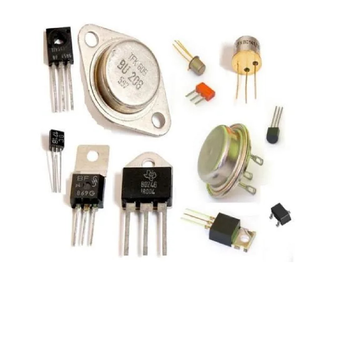
 Power Transistors
 Resistor & Smd & inductor
 Switches
 Aluminium Heat Sink
 Buzzer & Speaker
 capacitor
 Crystal Oscillators
 Doides
 Electric Fuses
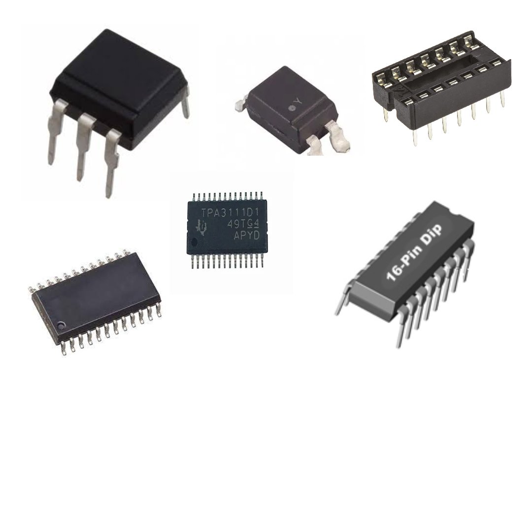
 ICs & Dips
 Power supply module
 Transformer
 Relay Module
 Kits
Kits Magnet
 RF Connectors
 PCT and DC Connectors
 Wires & Heat Shrink
 FFC, FPC, Berg connectors
 Nextion
 Segment
 Seedstudio
 Waveshare
 E Bike Batteries
 E bike Battery Case
 E bike Connectors
 E bike Display
 E bike Kit
 E bike Motors & Controllers
 Electronics Accessories
 Mechanical Accessories
 Display
 Cameras