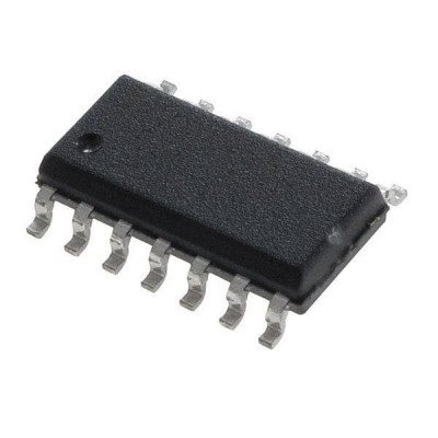
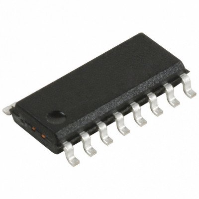
74HC40105 IC – (SMD Package) – 4-Bit x 16-Word FIFO Register IC (7440105)
The 74HC40105 is a first-in/first-out (FIFO) “elastic” storage register that can store 16 4-bit words. It can handle input and output data at different shifting rates. This feature makes it particularly useful as a buffer between asynchronous systems. Each word position in the register is clocked by a control flip-flop, which stores a marker bit. A logic 1 signifies that the data at that position is filled and a logic 0 denotes a vacancy in that position. The control flip-flop detects the state of the preceding flip-flop and communicates its own status to the succeeding flip-flop. When a control flip-flop is in the logic 0 state and sees a logic 1 in the preceding flip-flop, it generates a clock pulse. The clock pulse transfers data from the preceding four data latches into its own four data latches and resets the preceding flip-flop to logic 0. The first and last control flip-flops have buffered outputs. All empty locations “bubble” automatically to the input end, and all valid data ripples through to the output end. As a result, the status of the first control flip-flop (data-in ready output – DIR) indicates if the FIFO is full. The status of the last flip-flop (data-out ready output – DOR) indicates whether the FIFO contains data. As the earliest data is removed from the bottom of the data stack (output end), all data entered later will automatically ripple toward the output. Inputs include clamp diodes that enable the use of current limiting resistors to interface inputs to voltages in excess of VCC.
Apple Shopping Event
Hurry and get discounts on all Apple devices up to 20%
Sale_coupon_15
₹69.62
Inclusive of GST
- Pick up from the Robotwala Store
To pick up today
Free
- Shiprocket from Air
Our courier will deliver to the specified address
3-4 Days
139
- Shiprocket from Surface
courier will deliver to the specified address
5-7 Days
90
- Warranty 1 year
- Free 30-Day returns
Payment Methods:
Description
The 74HC40105 is a first-in/first-out (FIFO) “elastic” storage register that can store 16 4-bit words. It can handle input and output data at different shifting rates. This feature makes it particularly useful as a buffer between asynchronous systems. Each word position in the register is clocked by a control flip-flop, which stores a marker bit. A logic 1 signifies that the data at that position is filled and a logic 0 denotes a vacancy in that position. The control flip-flop detects the state of the preceding flip-flop and communicates its own status to the succeeding flip-flop. When a control flip-flop is in the logic 0 state and sees a logic 1 in the preceding flip-flop, it generates a clock pulse. The clock pulse transfers data from the preceding four data latches into its own four data latches and resets the preceding flip-flop to logic 0. The first and last control flip-flops have buffered outputs. All empty locations “bubble” automatically to the input end, and all valid data ripples through to the output end. As a result, the status of the first control flip-flop (data-in ready output – DIR) indicates if the FIFO is full. The status of the last flip-flop (data-out ready output – DOR) indicates whether the FIFO contains data. As the earliest data is removed from the bottom of the data stack (output end), all data entered later will automatically ripple toward the output. Inputs include clamp diodes that enable the use of current limiting resistors to interface inputs to voltages in excess of VCC.
Features :-
- Independent asynchronous inputs and outputs
- Expandable in either direction
- Reset capability
- Status indicators on inputs and outputs
- 3-state outputs
- CMOS input levels
- Complies with JEDEC standard JESD7A
- ESD protection:
HBM JESD22-A114F exceeds 2000 V
MM JESD22-A115-A exceeds 200 V
- Specified from -40 ?C to +85 ?C and from -40 ?C to +125 ?C
Specifications :-
|
Symbol |
Parameter |
Min |
Max |
Unit |
|
VCC |
Supply Voltage |
-0.5 |
+7 |
V |
|
IIK |
input clamping current |
– |
+20 |
mA |
|
Iok |
output clamping current |
– |
+20 |
mA |
|
IO |
output source or sink current |
– |
+25 |
mA |
|
ICC |
supply current |
– |
+50 |
mA |
|
IGND |
ground current |
-50 |
– |
mA |
|
Tstg |
storage temperature |
-65 |
+150 |
?C |
|
Ptot |
total power dissipation |
– |
500 |
mW |
Package Includes :-
1 X 74HC40105 IC – (SMD Package) – 4-Bit x 16-Word FIFO Register IC (7440105)
Additional information
Operating voltage | 2.5 3.0V |
Pixel Resolution | 0.3MP |
Photosensitive array | 640 x 480 |
Optical Size | 1.6 inch |
Angel of view | 67 degrees |
Maximum Frame Rate | 30fps VGA |
Sensitivity | 1.3V/(Lux-sec) |
Dormancy | Less than 20A |
Power consumption | 60mW/15fpsVGA YUV |
Temperature operation Range | -30 C ~ 70 C |
Pixel area | 3.6 x 3.6 m |
Signal to noise ratio (SNR) | 46 dB |
Dynamic range | 52 dB |






 Boards & Modules
 ARM Microcontroller
 AVR Microcontroller Board
 Arduino boards
 Advance Development Boards
 8051 Development Board
 Audio Amplifier Module
 Current & Volatage Sensor
 Breakout Board
 Flame Sensors
 Force Sensor
 Gas Sensors
 Hall Effect Sensor
 Humidity & Temperature Sensor
 LED Module
 PIR Sensor
 Pressure Sensors
 Proximity Sensor
 Relay Module
 Real Time Clock (RTC) Module
 Touch Sensor
 Ultrasonic Sensor
 Water Level & Water Flow Sensor
 Weighing Scale Sensor


 Ai Thinker ESp Wifi Module
 Pic Devlopment Board & programmer
 Led lights & Strips
 PCBs & Breadboard
 Potentiometer
 Power Transistors
 Resistor & Smd & inductor
 Switches
 Aluminium Heat Sink
 Buzzer & Speaker
 capacitor
 Crystal Oscillators
 Doides
 Electric Fuses
 ICs & Dips
 Power supply module
 Transformer
 Relay Module
 Kits
Kits Magnet
 RF Connectors
 PCT and DC Connectors
 Wires & Heat Shrink
 FFC, FPC, Berg connectors
 Nextion
 Segment
 Seedstudio
 Waveshare
 E Bike Batteries
 E bike Battery Case
 E bike Connectors
 E bike Display
 E bike Kit
 E bike Motors & Controllers
 Electronics Accessories
 Mechanical Accessories
 Display
 Cameras
Reviews
There are no reviews yet.