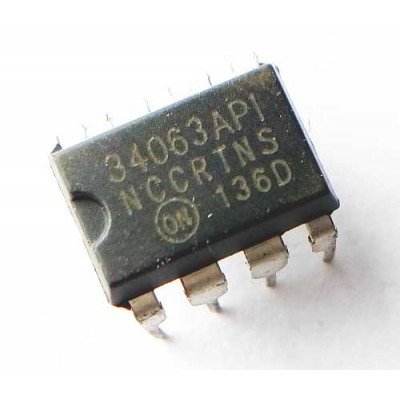
MC34151 High Speed Dual MOSFET Driver IC DIP-8 Package
The MC34151 is dual inverting high speed drivers specifically designed for applications that require low current digital circuitry to drive large capacitive loads with high slew rates. These devices feature low input current making them CMOS and LSTTL logic compatible, input hysteresis for fast output switching that is independent of input transition time, and two high current totem pole outputs ideally suited for driving power MOSFETs. Also included is an undervoltage lockout with hysteresis to prevent erratic system operation at low supply voltages. Typical applications include switching power supplies, dc to dc converters, capacitor charge pump voltage doublers/inverters, and motor controllers. The device is available in dual?in?line packages.
Apple Shopping Event
Hurry and get discounts on all Apple devices up to 20%
Sale_coupon_15
₹165.20
Inclusive of GST
- Pick up from the Robotwala Store
To pick up today
Free
- Shiprocket from Air
Our courier will deliver to the specified address
3-4 Days
139
- Shiprocket from Surface
courier will deliver to the specified address
5-7 Days
90
- Warranty 1 year
- Free 30-Day returns
Payment Methods:
Description
The MC34151 is dual inverting high speed drivers specifically designed for applications that require low current digital circuitry to drive large capacitive loads with high slew rates. These devices feature low input current making them CMOS and LSTTL logic compatible, input hysteresis for fast output switching that is independent of input transition time, and two high current totem pole outputs ideally suited for driving power MOSFETs. Also included is an undervoltage lockout with hysteresis to prevent erratic system operation at low supply voltages. Typical applications include switching power supplies, dc to dc converters, capacitor charge pump voltage doublers/inverters, and motor controllers. The device is available in dual?in?line packages.
Features:-
- Two Independent Channels with 1.5 A Totem Pole Output
- Output Rise and Fall Times of 15 ns with 1000 pF Load
- CMOS/LSTTL Compatible Inputs with Hysteresis
- Undervoltage Lockout with Hysteresis
- Low Standby Current
- Efficient High Frequency Operation
- Enhanced System Performance with Common Switching Regulator Control ICs
- Pin Out Equivalent to DS0026 and MMH0026
- These are Pb?Free and Halide?Free Devices
Specification:-
| Rating | Symbol | Value | Unit |
| Power Supply Voltage | VCC | 20 | V |
| Logic Input | VIN | ?0.3 to VCC | V |
| Gate Drive Output-Source Current | IO | 1.5 | A |
| Maximum Power Dissipation @ TA = 50?C | PD | 0.56 | W |
| Operating Junction Temperature | Tj | 150 | ?C |
| Operating Ambient Temperature | Ta | 0 to +70 | ?C |
| Storage Temperature Range | Tstg | ?65 to +150 | ?C |
| Human Body Model (HBM), Machine Model (MM), Charged Device Model (CDM) | ESD | 2000, 200, 1500 | V |
Related Document:-
Additional information
Operating voltage | 2.5 3.0V |
Pixel Resolution | 0.3MP |
Photosensitive array | 640 x 480 |
Optical Size | 1.6 inch |
Angel of view | 67 degrees |
Maximum Frame Rate | 30fps VGA |
Sensitivity | 1.3V/(Lux-sec) |
Dormancy | Less than 20A |
Power consumption | 60mW/15fpsVGA YUV |
Temperature operation Range | -30 C ~ 70 C |
Pixel area | 3.6 x 3.6 m |
Signal to noise ratio (SNR) | 46 dB |
Dynamic range | 52 dB |






 Boards & Modules
 ARM Microcontroller
 AVR Microcontroller Board
 Arduino boards
 Advance Development Boards
 8051 Development Board
 Audio Amplifier Module
 Current & Volatage Sensor
 Breakout Board
 Flame Sensors
 Force Sensor
 Gas Sensors
 Hall Effect Sensor
 Humidity & Temperature Sensor
 LED Module
 PIR Sensor
 Pressure Sensors
 Proximity Sensor
 Relay Module
 Real Time Clock (RTC) Module
 Touch Sensor
 Ultrasonic Sensor
 Water Level & Water Flow Sensor
 Weighing Scale Sensor


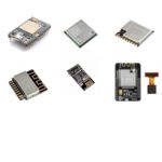 Ai Thinker ESp Wifi Module
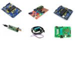 Pic Devlopment Board & programmer
 Led lights & Strips
 PCBs & Breadboard
 Potentiometer
 Power Transistors
 Resistor & Smd & inductor
 Switches
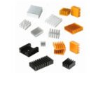 Aluminium Heat Sink
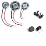 Buzzer & Speaker
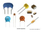 capacitor
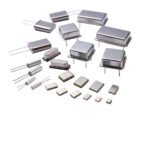 Crystal Oscillators
 Doides
 Electric Fuses
 ICs & Dips
 Power supply module
 Transformer
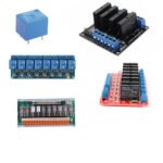 Relay Module
 Kits
Kits Magnet
 RF Connectors
 PCT and DC Connectors
 Wires & Heat Shrink
 FFC, FPC, Berg connectors
 Nextion
 Segment
 Seedstudio
 Waveshare
 E Bike Batteries
 E bike Battery Case
 E bike Connectors
 E bike Display
 E bike Kit
 E bike Motors & Controllers
 Electronics Accessories
 Mechanical Accessories
 Display
 Cameras
Reviews
There are no reviews yet.