Showing 217–228 of 700 results
ICs & Dips
74LS132 IC – (SMD Package) Quad 2-Input Schmitt Trigger IC (74132 IC)
₹28.32
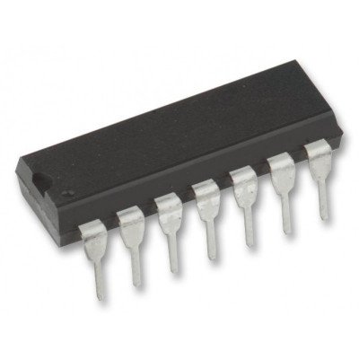
74LS132 Quad 2-Input Schmitt Trigger IC (74132 IC) DIP-14 Package
₹38.94
74LS138 1-of-8 Decoder/Demultiplexer IC (74138) DIP-16 Package
₹53.10
These Schottky-clamped circuits are designed to be used in high-performance memory-decoding or data-routing applications, requiring very short propagation delay times. In high-performance memory systems these decoders can be used to minimize the effects of system decoding. When used with high-speed memories, the delay times of these
74LS138 IC – (SMD Package) 1-to-8 Decoder/Demultiplexer IC (74138 IC)
₹46.02
These Schottky-clamped circuits are designed to be used in high-performance memory-decoding or data-routing applications, requiring very short propagation delay times. In high-performance memory systems these decoders can be used to minimize the effects of system decoding. When used with high-speed memories, the delay times of these decoders are usually less than the typical access time of the memory. This means that the effective system delay introduced by the decoder is negligible. The 74LS138 decodes one-of-eight lines, based upon the conditions at the three binary select inputs and the three enable inputs. Two active-low and one active-high enable inputs reduce the need for external gates or inverters when expanding. A 24-line decoder can be implemented with no external inverters, and a 32-line decoder requires only one inverter. An enable input can be used as a data input for demultiplexing applications.
74LS139 Dual 2-to-4 line Decoder/Demultiplexer IC (74139 IC) DIP-16 Package
₹29.50
The 74LS139 comprises two separate two-line-to-four line decoders in a single package. The active-low enable input can be used as a data line in demultiplexing applications. All of these decoders/demultiplexers feature fully buffered inputs, presenting only one normalized load to its driving circuit. All inputs are clamped with high-performance Schottky diodes to suppress line-ringing and simplify system design.
74LS139 IC – (SMD Package) – High Speed Dual 1-of-4 Decoder/De-multiplexer IC (74139 IC)
₹34.22
The 74LS139 is a clamped circuits are designed to be used in high-performance memory-decoding or data-routing applications, requiring very short propagation delay times. In high-performance memory systems these decoders can be used to minimize the effects of system decoding. When used with high-speed memories, the delay times of these decoders are usually less than the typical access time of the memory. This means that the effective system delay introduced by the decoder is negligible. Two active-low and one active-high enable inputs reduce the need for external gates or inverters when expanding. A 24-line decoder can be implemented with no external inverters, and a 32-line decoder requires only one inverter. An enable input can be used as a data input for demultiplexing applications. The 74LS139 comprises two separate two-line-to-fourline decoders in a single package. The active-low enable input can be used as a data line in demultiplexing applications. All of these decoders/demultiplexers feature fully buffered inputs, presenting only one normalized load to its driving circuit. All inputs are clamped with high-performance Schottky diodes to suppress line-ringing and simplify system design.
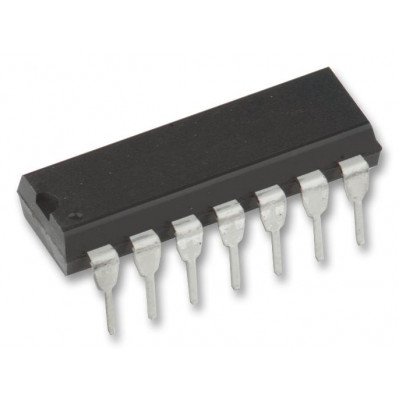
74LS14 Hex Schmitt Trigger Inverter IC (7414 IC) DIP-14 Package
₹17.70
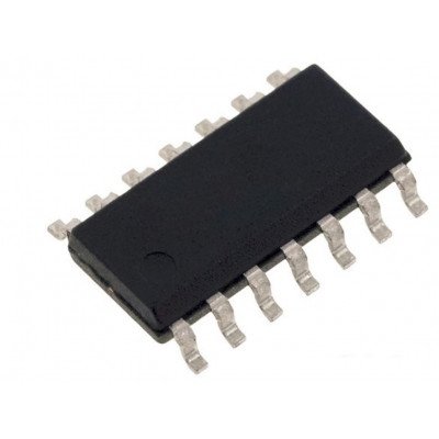
74LS14 IC – (SMD Package) Hex Schmitt Trigger Inverter IC (7414 IC)
₹29.50
74LS147 Decimal to BCD Priority Encoder IC (74147 IC) DIP-16 Package
₹62.54
The 74LS147 TTL encoders feature priority decoding of the inputs to ensure that only the highest-order data line is encoded. The ?147 and ?LS147 devices encode nine data lines to four-line (8-4-2-1) BCD. The implied decimal zero condition requires no input condition, as zero is encoded when all nine data lines are at a high logic level. Cascading circuitry (enable input EI and enable output EO) has been provided to allow octal expansion without the need for external circuitry. For all types, data inputs and outputs are active at the low logic level.
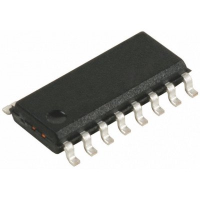
74LS15 IC – (SMD Package) Triple 3-InputT AND Gate IC (7415 IC)
₹28.32
The 74LS15 is a three-input positive-AND gate IC with three separate inputs built in low-power. The logic AND function is performed by each of the three separate gates in this device. They use positive logic to perform the Boolean functions Y = A ? B ? C. This IC is designed to operate at temperatures ranging from 55?C to 125?C, which is the complete military temperature range. The 74HC logic family is pin-out compatible with the 74LS logic family of high grade. It features a 4.5V to 5.5V supply voltage range. The 74LS15 has a strong noise immunity and, as a result, can drive TTL loads. Internal diode clamps to VCC and ground protect all inputs from static discharge damage. The AND gate designed as a basic digital logic gate that implements logical conjunction. An AND gate operates on logical multiplication rules. If all the inputs to the AND gate are HIGH, then the output will be high. If none or not all inputs to the AND gate are HIGH, results in LOW output.
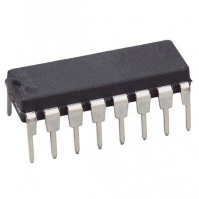
74LS151 8-Input Digital Multiplexer IC (74151) DIP-16 Package
₹53.10
This data selector/multiplexer contains full on-chip decoding to select the desired data source. The 74LS151 selects one-of-eight data sources. The 74LS151 has a strobe input which must be at a low logic level to enable these devices. A high level at the strobe forces the W output HIGH, and the Y output LOW. The 74LS151 features complementary W and Y outputs.







 Boards & Modules
 ARM Microcontroller
 AVR Microcontroller Board
 Arduino boards
 Advance Development Boards
 8051 Development Board
 Audio Amplifier Module
 Current & Volatage Sensor
 Breakout Board
 Flame Sensors
 Force Sensor
 Gas Sensors
 Hall Effect Sensor
 Humidity & Temperature Sensor
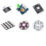 LED Module
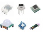 PIR Sensor
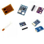 Pressure Sensors
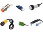 Proximity Sensor
 Relay Module
 Real Time Clock (RTC) Module
 Touch Sensor
 Ultrasonic Sensor
 Water Level & Water Flow Sensor
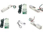 Weighing Scale Sensor




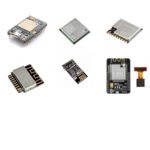 Ai Thinker ESp Wifi Module
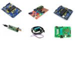 Pic Devlopment Board & programmer
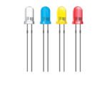 Led lights & Strips
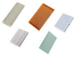 PCBs & Breadboard
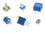 Potentiometer
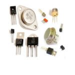 Power Transistors
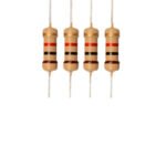 Resistor & Smd & inductor
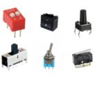 Switches
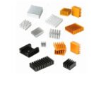 Aluminium Heat Sink
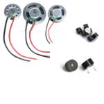 Buzzer & Speaker
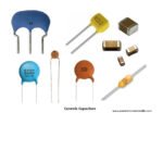 capacitor
 Crystal Oscillators
 Doides
 Electric Fuses
 ICs & Dips
 Power supply module
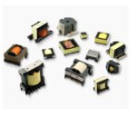 Transformer
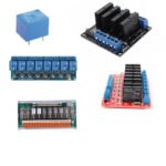 Relay Module
 Kits
Kits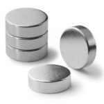 Magnet
 RF Connectors
 PCT and DC Connectors
 Wires & Heat Shrink
 FFC, FPC, Berg connectors
 Nextion
 Segment
 Seedstudio
 Waveshare
 E Bike Batteries
 E bike Battery Case
 E bike Connectors
 E bike Display
 E bike Kit
 E bike Motors & Controllers
 Electronics Accessories
 Mechanical Accessories
 Display
 Cameras