

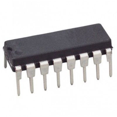
CD4082 Dual 4 Input AND Gate IC DIP-14 Package
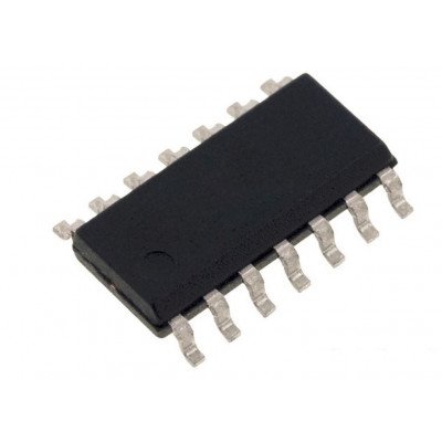
CD4093 IC – (SMD Package) – Quad 2-Input NAND Schmitt Trigger IC
The CD4093 consists of four Schmitt-trigger circuits. Each circuit functions as a 2-input NAND gate with Schmitttrigger action on both inputs. The gate switches at different points for positive and negative-going signals. The difference between the positive (VT +) and the negative voltage (VT ?) is defined as hysteresis voltage (VH). All outputs have equal source and sink currents and conform to standard B-series output drive.

CD4093 Quad 2-Input NAND Schmitt Trigger IC DIP-14 Package
CD4093 consists of four Schmitt-trigger circuits. Each circuit functions as a two-input NAND gate with Schmitt-trigger action on both inputs. The gate switches at different points for positive- and negative-going signals. The difference between the positive voltage (VP) and the negative voltage (VN) is defined as hysteresis voltage (VH) (see Fig. 2).

CD4094 8-Stage Shift and Store Bus Register IC DIP-16 Package
CD4094 is a 8-stage serial shift register having a storage
latch associated with each stage for strobing data from the serial
input to parallel buffered 3-state outputs. The parallel outputs
may be connected directly to common bus lines. Data is shifted
on positive clock transitions. The data in each shift register stage
is transferred to the storage register when the STROBE input is
high. Data in the storage register appears at the outputs whenever
the OUTPUT-ENABLE signal is high.

CD4099 8 bit Addressable Latch IC DIP-16 Package
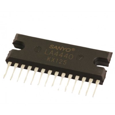
CD4440 / LA4440 6W 2-Channel Audio Power Amplifier IC SIP14H Package
CD4440 / LA4440 is a Stereotype audio amplifier IC with an inbuilt dual channel that enables it for stereo and bridge amplification applications. It gives 6W output in dual mode and 19W in bridge mode. This IC has inbuilt over power protection, small residual noise, good ripple rejection and special feature of pin-to-pin protection.

CD4504 Hex Voltage Level Shifter IC DIP-16 Package
CD4504 hex voltage level-shifter consists of six circuits which shift input signals from the VCC logic level to the VDD logic level. To shift TTL signals to CMOS logic levels, the SELECT input is at the VCC HIGH logic state. When the SELECT input is a LOW logic state, each circuit translates signals from one CMOS level to another.

CD4511 BCD To 7 Segment Latch Decoder Driver IC DIP-16 Package
CD4511 types are BCD-to-7-segment latch decoder drivers constructed with CMOS logic and n-p-n bipolar transistor output devices on a single monolithic structure. These devices combine the low quiescent power dissipation and high noise immunity features of RCA CMOS with n-p-n bipolar output transistors capable of sourcing up to 25 MA. This capability allows the CD4511 types to drive LED's and other displays directly.
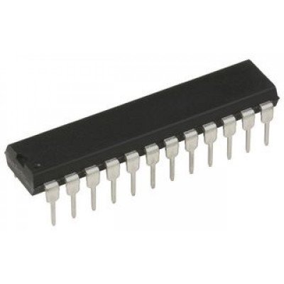
CD4514 4 Bit Latch/4-16 Line Decoder IC DIP-24 Package
The CD4514 is 4-to-16 line decoders with latched inputs implemented with complementary MOS (CMOS) circuits constructed with N- and P-channel enhancement mode transistors. These circuits are primarily used in decoding applications where low power dissipation and/or high noise immunity is required. The CD4514 (output active high option) presents a logical ?1? at the selected output. The input latches are R?S type flip-flops, which hold the last input data presented prior to the strobe transition from ?1? to ?0?. This input data is decoded and the corresponding output is activated. An output inhibit line is also available.
CD4518 Dual BCD Up Counter IC DIP-16 Package
CD4518 consist of two identical, internally synchronous 4-stage counters. The counter stages are D-type flip-flops having interchangeable CLOCK and ENABLE lines for incrementing on either the positive-going or negative-going transition. For single-unit operation the ENABLE input is maintained high and the counter advances on each positive-going transition of the CLOCK. The counters are cleared by high levels on their RESET lines. The counter can be cascaded in the ripple mode by connecting Q4 to the enable input of the subsequent counter while the CLOCK input of the latter is held low. The CD4518 types are supplied in 16-lead hermetic dual-in-line ceramic packages (F3A suffix), 16-lead dual-in-line plastic packages (E suffix), 16-lead small-outline packages (M, M96, and NSR suffixes), and 16-lead thin shrink small-outline packages (PW and PWR suffixes).


CD4532 8 Bit Priority Encoder IC DIP-16 Package
CD4532 consists of combinational logic that encodes the highest priority input (D7-D0) to a 3-bit binary code. The eight inputs, D7 through D0, each have an assigned priority; D7 is the highest priority and D0 is the lowest. The priority encoder is inhibited when the chip-enable input EI is low. When EI is high, the binary representation of the highest-priority input appears on output lines Q2-Q0, and the group select line GS is high to indicate that priority inputs are present. The enable-out (EO) is high when no priority inputs are present. If any one input is high, EO is low and all cascaded lower-order stages are disabled.

 Boards & Modules
 ARM Microcontroller
 AVR Microcontroller Board
 Arduino boards
 Advance Development Boards
 8051 Development Board
 Audio Amplifier Module
 Current & Volatage Sensor
 Breakout Board
 Flame Sensors
 Force Sensor
 Gas Sensors
 Hall Effect Sensor
 Humidity & Temperature Sensor
 LED Module
 PIR Sensor
 Pressure Sensors
 Proximity Sensor
 Relay Module
 Real Time Clock (RTC) Module
 Touch Sensor
 Ultrasonic Sensor
 Water Level & Water Flow Sensor
 Weighing Scale Sensor


 Ai Thinker ESp Wifi Module
 Pic Devlopment Board & programmer
 Led lights & Strips
 PCBs & Breadboard
 Potentiometer
 Power Transistors
 Resistor & Smd & inductor
 Switches
 Aluminium Heat Sink
 Buzzer & Speaker
 capacitor
 Crystal Oscillators
 Doides
 Electric Fuses
 ICs & Dips
 Power supply module
 Transformer
 Relay Module
 Kits
Kits Magnet
 RF Connectors
 PCT and DC Connectors
 Wires & Heat Shrink
 FFC, FPC, Berg connectors
 Nextion
 Segment
 Seedstudio
 Waveshare
 E Bike Batteries
 E bike Battery Case
 E bike Connectors
 E bike Display
 E bike Kit
 E bike Motors & Controllers
 Electronics Accessories
 Mechanical Accessories
 Display
 Cameras