
CNY74-4 IC – 4-Channel Optocoupler with Phototransistor IC
The CNY74-4 consist of a photo transistor optically coupled to a gallium arsenide infrared-emitting diode in an 8-lead, resp. 16-lead plastic dual inline package. The elements are mounted on one lead frame using a co planar technique, providing a fixed distance between input and output for highest safety requirements.

CP2102 (SMD QFN-28 Package) USB to UART Bridge Controller IC

CS5460A-BS IC – (SMD SSOP-24 Package) – Single Phase Bi-Directional Power/Energy IC
The CS5460A is a highly integrated power measurement solution which combines two Analog-to-digital Converters (ADCs), high-speed power calculation functions, and a serial interface on a single chip. It is designed to accurately measure and calculate: Real (True) Energy, Instantaneous Power, IRMS, and VRMS for single phase 2- or 3-wire power metering applications. The CS5460A interfaces to a low-cost shunt resistor or transformer to measure current, and to a resistive divider or potential transformer to measure voltage. The CS5460A features a bi-directional serial interface for communication with a microcontroller and a pulse output engine for which the average pulse frequency is proportional to the real power. The CS5460A has on-chip functionality to facilitate AC or DC system-level calibration. The ?Auto-boot? feature allows the CS5460A to function ?stand-alone? and to initialize itself on system power-up. In Auto-boot Mode, the CS5460A reads the calibration data and start-up instructions from an external EEPROM. In this mode, the CS5460A can operate without a microcontroller, in order to lower the total bill-of-materials cost.
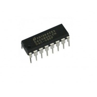
DAC0800 8-Bit Digital to Analog D/A Converter IC DIP-16 Package
The DAC0800 series are monolithic 8-bit high-speed current-output digital-to-analog converters (DAC) featuring typical settling times of 100 ns. When used as a multiplying DAC, monotonic performance over a 40 to 1 reference current range is possible. The DAC0800 series also features high compliance complementary current outputs to allow differential output voltages of 20 Vp-p with simple resistor loads. The reference-to-full-scale current matching of better than ?1 LSB eliminates the need for full-scale trims in most applications, while the non linearities of better than ?0.1% over temperature minimizes system error accumulations.

DAC0808 8-Bit Digital to Analog D/A Converter IC DIP-16 Package
The DAC0808 is an 8-bit monolithic digital-to-analog converter (DAC) featuring a full scale output current settling time of 150 ns while dissipating only 33 mW with ?5V supplies. No reference current (IREF) trimming is required for most applications since the full scale output current is typically ?1 LSB of 255 IREF/256. Relative accuracies of better than ?0.19% assure 8-bit monotonicity and linearity while zero level output current of less than 4 ?A provides 8-bit zero accuracy for IREF>=2 mA. The power supply currents of the DAC0808 is independent of bit codes, and exhibits essentially constant device characteristics over the entire supply voltage range.

DG201 IC – (SMD Package) – Quad CMOS Analog Switches IC
DG408D IC – Improved, 8-Channel/Dual 4-Channel, CMOS Analog Multiplexer IC
The DG408 analog multiplexers now feature guaranteed matching between channels (8? max) and flatness over the specified signal range (9? max). These low on-resistance muxes (100? max) conduct equally well in either direction and feature guaranteed low charge injection (15pC max). In addition, these new muxes offer low input off-leakage current over temperature?less than 5nA at +85?C. The DG408 is a 1-of-8 multiplexer/demultiplexer. The muxes operate with a +5V to +30V single supply and with ?5V to ?20V dual supplies. ESD protection is guaranteed to be greater than 2000V per Method 3015.7 of MIL-STD-883. These improved muxes is pin-compatible plug-in upgrades for the industry standard DG408.
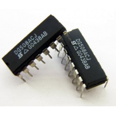
DG508 IC – CMOS Analog Multiplexer IC
The DG508 is an 8-channel single-ended analog multiplexer designed to connect one of eight inputs to a common output as determined by a 3-bit binary address (A0, A1, A2). Break-before-make switching action protects against momentary cross talk between adjacent channels. An on channel conducts current equally well in both directions. In the off state each channel blocks voltages up to the power supply rails. An enable (EN) function allows the user to reset the multiplexer / demultiplexer to all switches off for stacking several devices. All control inputs, addresses (AX) and enable (EN) are TTL compatible over the full specified operating temperature range. The DG508B is fabricated on an enhanced SG-II CMOS process that achieves improved performance on: reduced charge injection, lower device leakage, and minimized parasitic capacitance. As the DG508 has a long history in the industry with many suppliers offering copies - and in some cases improved variations - with the best in class improvements. Applications for the DG508B include high speed and high precision data acquisition, audio signal switching and routing, ATE systems, and avionics. High performance and low power dissipation make them ideal for battery operated and remote instrumentation applications. The DG508B have the absolute maximum voltage rating extended to 44 V. Additionally, single supply operation is also allowed. An epitaxial layer prevents latch-up. The DG508B is both available in 16-lead SOIC, TSSOP, PDIP, and mini QFN (1.8 mm x 2.6 mm) package options with extended temperature range of -40 ?C to +125 ?C.
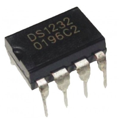
DS1232 IC – Micro Monitor Chip IC
The DS1232 Micro Monitor? Chip monitors three vital conditions for a microprocessor: power supply, software execution, and external override. First, a precision temperature-compensated reference and comparator circuit monitors the status of VCC. When an out-of-tolerance condition occurs, an internal power fail signal is generated which forces reset to the active state. When VCC returns to an in-tolerance condition, the reset signals are kept in the active state for a minimum of 250 ms to allow the power supply and processor to stabilize.
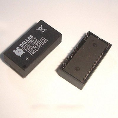
DS12C887 IC – Real Time Clock (RTC) IC
RTC DS 12C887 is widely used to provide exact time and date in many applications such as x86 IBM PC. This RTC provides time components hour, minute and second in addition to the date/calendar components of year, month and day. This chip uses an internal lithium battery, which keeps the time and date updated even when the power is off. The DS12C887 works on CMOS technology to keep the power consumption low. It has a total of 128 bytes of non volatile RAM. It uses 14 bytes of RAM for storing the values of clock/calendar and control registers. The rest 114 bytes of RAM are for general purpose data storage.
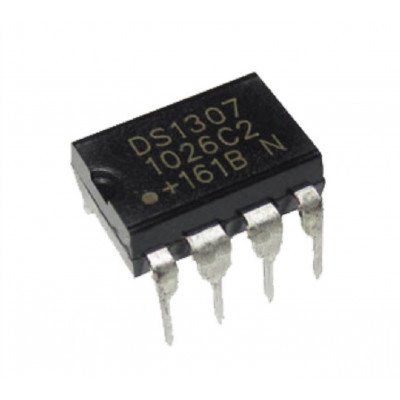
DS1307 IC – Real Time Clock (RTC) IC
The DS1307 Serial Real-Time Clock is a low-power, full binary-coded decimal (BCD) clock/calendar plus 56 bytes of NV SRAM. Address and data are transferred serially via a 2-wire, bi-directional bus. The clock/calendar provides seconds, minutes, hours, day, date, month, and year information. The end of the month date is automatically adjusted for months with fewer than 31 days, including corrections for leap year. The clock operates in either the 24-hour or 12-hour format with AM/PM indicator. The DS1307 has a built-in power sense circuit that detects power failures and automatically switches to the battery supply.

 Boards & Modules
 ARM Microcontroller
 AVR Microcontroller Board
 Arduino boards
 Advance Development Boards
 8051 Development Board
 Audio Amplifier Module
 Current & Volatage Sensor
 Breakout Board
 Flame Sensors
 Force Sensor
 Gas Sensors
 Hall Effect Sensor
 Humidity & Temperature Sensor
 LED Module
 PIR Sensor
 Pressure Sensors
 Proximity Sensor
 Relay Module
 Real Time Clock (RTC) Module
 Touch Sensor
 Ultrasonic Sensor
 Water Level & Water Flow Sensor
 Weighing Scale Sensor


 Ai Thinker ESp Wifi Module
 Pic Devlopment Board & programmer
 Led lights & Strips
 PCBs & Breadboard
 Potentiometer
 Power Transistors
 Resistor & Smd & inductor
 Switches
 Aluminium Heat Sink
 Buzzer & Speaker
 capacitor
 Crystal Oscillators
 Doides
 Electric Fuses
 ICs & Dips
 Power supply module
 Transformer
 Relay Module
 Kits
Kits Magnet
 RF Connectors
 PCT and DC Connectors
 Wires & Heat Shrink
 FFC, FPC, Berg connectors
 Nextion
 Segment
 Seedstudio
 Waveshare
 E Bike Batteries
 E bike Battery Case
 E bike Connectors
 E bike Display
 E bike Kit
 E bike Motors & Controllers
 Electronics Accessories
 Mechanical Accessories
 Display
 Cameras