


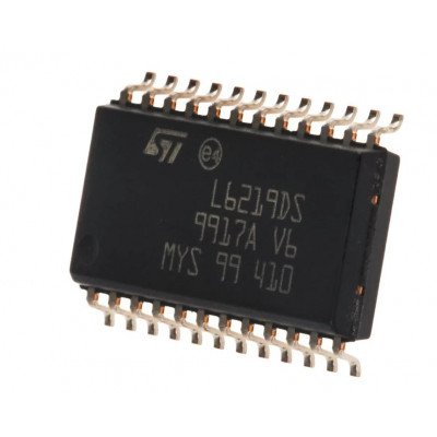
L6219 IC – (SMD Package) – Stepper Motor Driver IC
The L6219 is a bipolar monolithic integrated circuits intended to control and drive both winding of a bipolar stepper motor or bidirectionally control two DC motors. The L6219 with a few external components form a complete control and drive circuit for LS-TTL or microprocessor controlled stepper motor system. The power stage is a dual full bridge capable of sustaining 46 V and including four diodes for current recirculation. A cross conduction protection is provided to avoid simultaneous cross conduction during switching current direction. An internal pulse-width-modulation (PWM) controls the output current to 750 mA with peak startup current up to 1 A. Wide range of current control from 750 mA (each bridge) is permitted by means of two logic inputs and an external voltage reference. A phase input to each bridge determines the load current direction. A thermal protection circuitry disables the outputs if the chip temperature exceeds safe operating limits.

L6219 Stepper Motor Driver IC DIP-24 Package
The L6219 is a bipolar monolithic integrated circuits intended to control and drive both winding of a bipolar stepper motor or bidirectionally control two DC motors. The L6219 with a few external components form a complete control and drive circuit for LS-TTL or microprocessor controlled stepper motor system. The power stage is a dual full bridge capable of sustaining 46 V and including four diodes for current recirculation. A cross conduction protection is provided to avoid simultaneous cross conduction during switching current direction. An internal pulse-width-modulation (PWM) controls the output current to 750 mA with peak startup current up to 1 A. Wide range of current control from 750 mA (each bridge) is permitted by means of two logic inputs and an external voltage reference. A phase input to each bridge determines the load current direction. A thermal protection circuitry disables the outputs if the chip temperature exceeds safe operating limits.
L6565 IC – (SMD Package) – Quasi-Resonant SMPS Controller IC

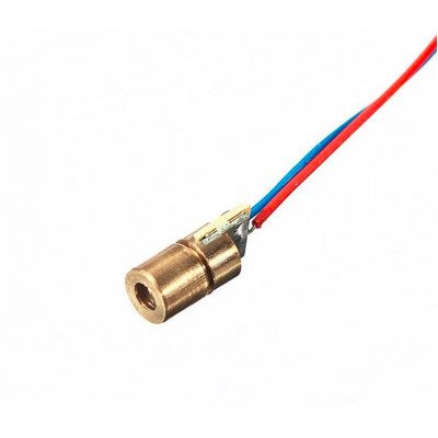
Laser Diode – Red – 650nm – (3V to 5V) – 6mm – 5mW

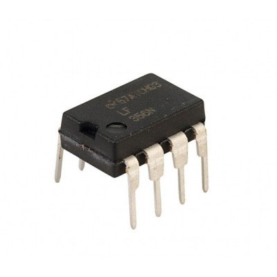
LF351 Wide Bandwidth JFET Input Op-Amp IC DIP-8 Package
The LF351 is a low cost high speed JFET input operational amplifier with an internally trimmed input offset voltage (BI-FET IITM technology). The device requires a low supply current and yet maintains a large gain bandwidth product and a fast slew rate. In addition, well matched high voltage JFET input devices provide very low input bias and offset currents. The LF351 is pin compatible with the standard LM741 and uses the same offset voltage adjustment circuitry. This feature allows designers to immediately upgrade the overall performance of existing LM741 designs. The LF351 may be used in applications such as high speed integrators, fast D/A converters, sample-and-hold circuits and many other circuits requiring low input offset voltage, low input bias current, high input impedance, high slew rate and wide bandwidth. The device has low noise and offset voltage drift, but for applications where these requirements are critical, the LF356 is recommended. If maximum supply current is important, however, the LF351 is the better choice.

LF353 Wide Bandwidth Dual JFET Input Op-Amp IC DIP-8 Package
This LF353 device is a low-cost, high-speed, JFET input operational amplifier with very low input offset voltage. It requires low supply current yet maintains a large gain-bandwidth product and a fast slew rate. In addition, the matched high-voltage JFET input provides very low input bias and offset currents. The LF353 can be used in applications such as high speed integrators, digital-to-analog converters, sample-and-hold circuits, and many other circuits. The LF353 is characterized for operation from 0?C to 70?C.
LF356 JFET Input Op-Amp IC DIP-8 Package
The LF356 device are the first monolithic JFET input operational amplifiers to incorporate well matched, high-voltage JFETs on the same chip with standard bipolar transistors (BI-FET? Technology). These amplifiers feature low input bias and offset currents/low offset voltage and offset voltage drift, coupled with offset adjust, which does not degrade drift or common-mode rejection. The devices are also designed for high slew rate, wide bandwidth, extremely fast settling time, low voltage and current noise and a low 1/f noise corner.
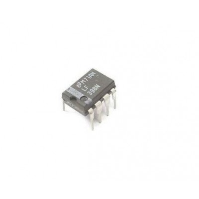
LF398 Sample and Hold Amplifier IC DIP-8 Package
The LF398 devices are monolithic sample-and-hold circuits that use BI-FET technology to obtain ultrahigh DC accuracy with fast acquisition of signal and low droop rate. Operating as a unity-gain follower, DC gain accuracy is 0.002% typical and acquisition time is as low as 6 ?s to 0.01%. A bipolar input stage is used to achieve low offset voltage and wide bandwidth. Input offset adjust is accomplished with a single pin and does not degrade input offset drift. The wide bandwidth allows the LF398 to be included inside the feedback loop of 1-MHz operational amplifiers without having stability problems. Input impedance of 1010 ? allows high-source impedances to be used without degrading accuracy. P-channel junction FETs are combined with bipolar devices in the output amplifier to give droop rates as low as 5 mV/min with a 1-?F hold capacitor. The JFETs have much lower noise than MOS devices used in previous designs and do not exhibit high temperature instabilities. The overall design ensures no feed through from input to output in the hold mode, even for input signals equal to the supply voltages. Logic inputs on the LF398 are fully differential with low input current, allowing for direct connection to TTL, PMOS, and CMOS. Differential threshold is 1.4 V. The LF398 will operate from ?5-V to ?18-V supplies. An A version is available with tightened electrical specifications.

LF412 Dual JFET Input Operational Amplifier IC DIP-8 Package
The LF412 devices are low cost, high speed, JFET input operational amplifiers with very low input offset voltage and input offset voltage drift. They require low supply current yet maintain a large gain bandwidth product and fast slew rate. In addition, well matched high voltage JFET input devices provide very low input bias and offset currents. The LF412 dual is pin compatible with the LM1558, allowing designers to immediately upgrade the overall performance of existing designs.

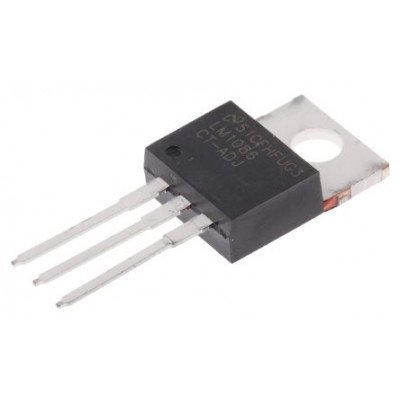
LM1085-ADJ (LM1085) – 3A Adjustable Low Dropout (LDO) Positive Voltage Regulator

 Boards & Modules
 ARM Microcontroller
 AVR Microcontroller Board
 Arduino boards
 Advance Development Boards
 8051 Development Board
 Audio Amplifier Module
 Current & Volatage Sensor
 Breakout Board
 Flame Sensors
 Force Sensor
 Gas Sensors
 Hall Effect Sensor
 Humidity & Temperature Sensor
 LED Module
 PIR Sensor
 Pressure Sensors
 Proximity Sensor
 Relay Module
 Real Time Clock (RTC) Module
 Touch Sensor
 Ultrasonic Sensor
 Water Level & Water Flow Sensor
 Weighing Scale Sensor


 Ai Thinker ESp Wifi Module
 Pic Devlopment Board & programmer
 Led lights & Strips
 PCBs & Breadboard
 Potentiometer
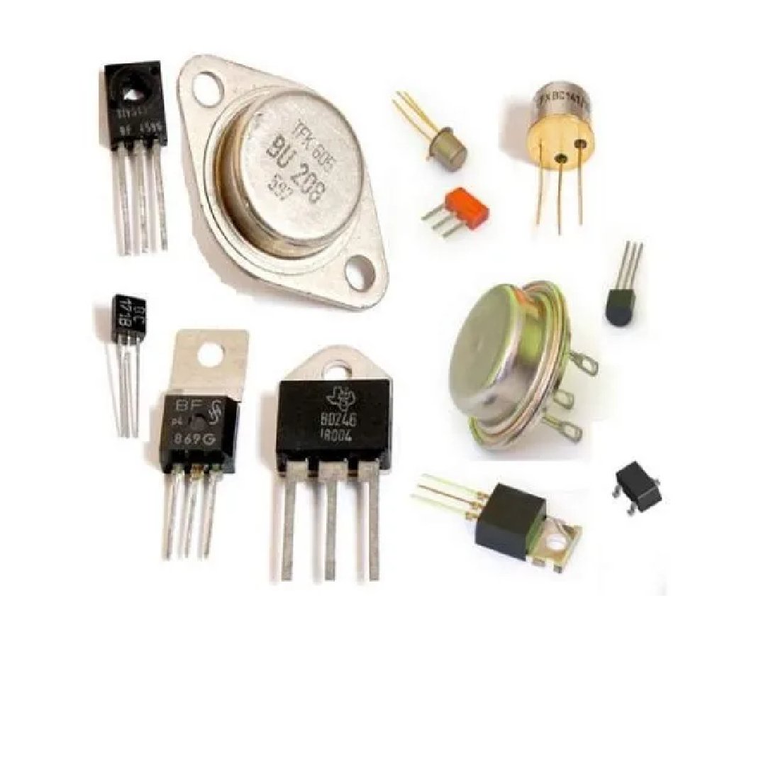
 Power Transistors
 Resistor & Smd & inductor
 Switches
 Aluminium Heat Sink
 Buzzer & Speaker
 capacitor
 Crystal Oscillators
 Doides
 Electric Fuses
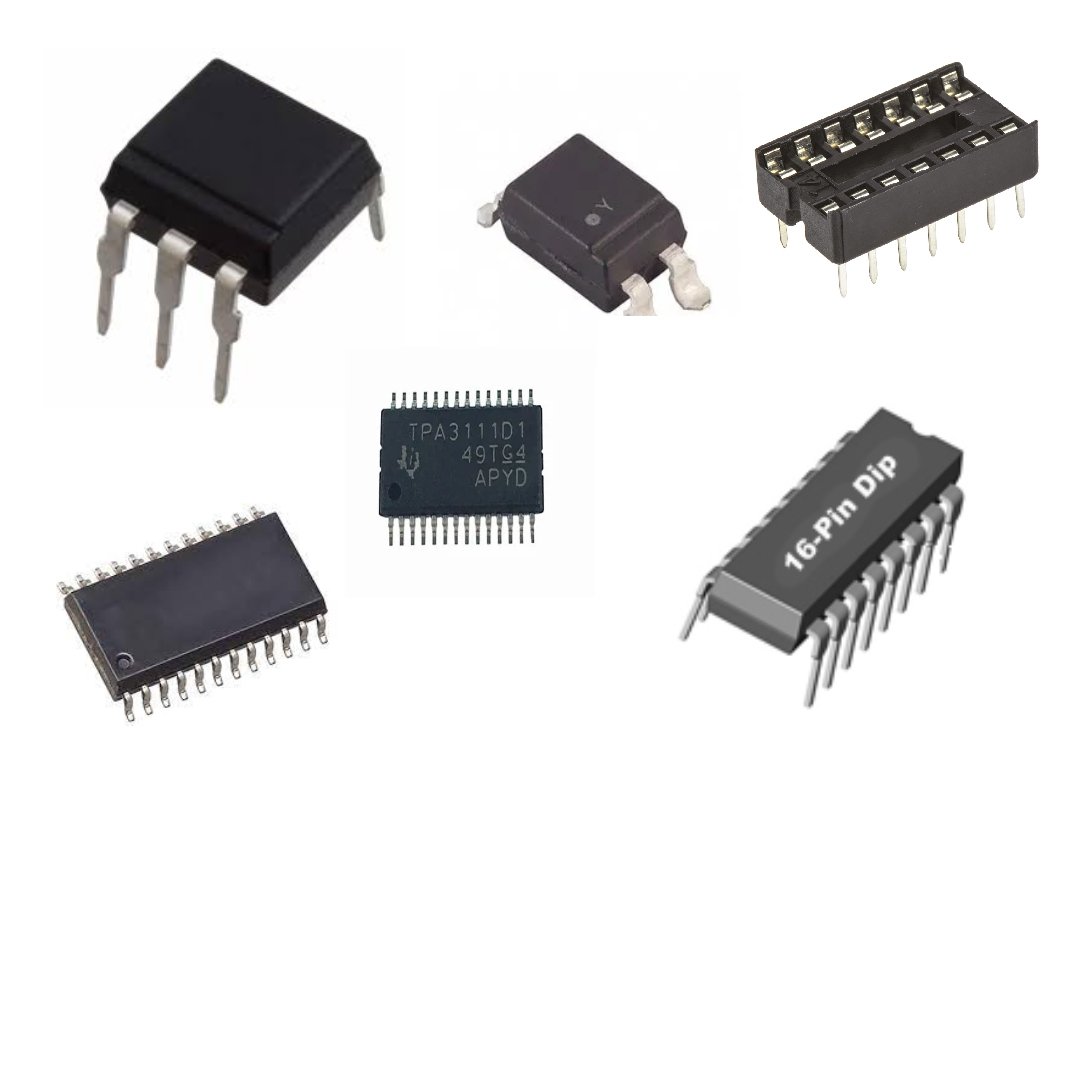
 ICs & Dips
 Power supply module
 Transformer
 Relay Module
 Kits
Kits Magnet
 RF Connectors
 PCT and DC Connectors
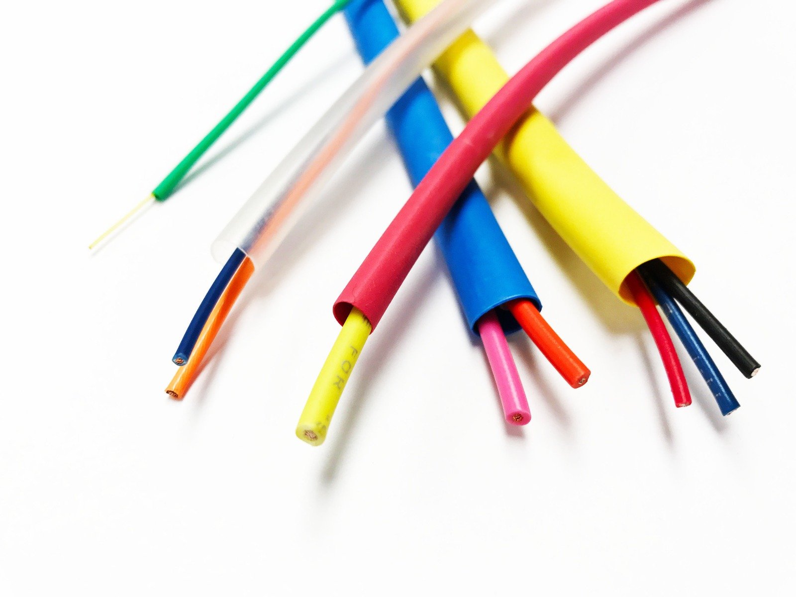
 Wires & Heat Shrink
 FFC, FPC, Berg connectors
 Nextion
 Segment
 Seedstudio
 Waveshare
 E Bike Batteries
 E bike Battery Case
 E bike Connectors
 E bike Display
 E bike Kit
 E bike Motors & Controllers
 Electronics Accessories
 Mechanical Accessories
 Display
 Cameras