


74LS05 Hex Inverters with Open Collector IC (7405) DIP-14 Package

74LS05 IC – (SMD Package) Hex Inverters with Open-Collector IC (7405 IC)
74LS06 Hex Inverter Buffer IC (7406 IC) DIP-14 Package
This 74LS06 monolithic hex inverter buffers/drivers feature high-voltage open-collector outputs to interface with high-level circuits (such as MOS), or for driving high-current loads, and are also characterized for use as inverter buffers for driving TTL inputs. The ?LS06 has a rated output voltage of 30 V and the ?LS16 has a rated output voltage of 15 V. The maximum sink current for the 74LS06 is 40 mA. The circuits is compatible with most TTL families. Inputs are diode-clamped to minimize transmission-effects, which simplifies design. Typical power dissipation is 175 mW and average propagation delay time is 8 ns. The 74LS06 is characterized for operation from 0?C to 70?C.
74LS06 IC – (SMD Package) – Hex Inverter -Buffer IC (7406 IC)
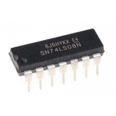
74LS08 Quadruple 2-Input Positive AND Gate IC (7408) DIP-14 Package

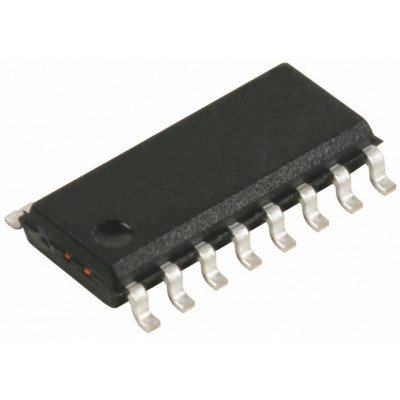
74LS10 IC – (SMD Package) – Triple 3-Input NAND Gates IC (7410 IC)

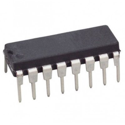
74LS109 Dual J-K Positive Edge-Triggered Flip-Flop IC (74109 IC) DIP-16 Package
The 74LS109 devices contain two independent J-K positive-edge-triggered flip-flops. A low level at the preset or clear inputs sets or resets the outputs regardless of the levels of the other inputs. When preset and clear are inactive (high), data at the J and K inputs meeting the setup time requirements are transferred to the outputs on the positive-going edge of the clock pulse. Clock triggering occurs at a voltage level and is not directly related to the rise time of the clock pulse. Following the hold time interval, data at the J and K inputs may be changed without affecting the levels at the outputs. These versatile flip-flops can perform as toggle flip-flops by grounding K and tying J high. They also can perform as D-type flip-flops if J and K are tied together.
74LS109 IC – (SMD Package) Dual J-K Positive Edge-Triggered Flip-Flop IC (74109 IC)
The 74LS109 devices contain two independent J-K positive-edge-triggered flip-flops. A low level at the preset or clear inputs sets or resets the outputs regardless of the levels of the other inputs. When preset and clear are inactive (high), data at the J and K inputs meeting the setup time requirements are transferred to the outputs on the positive-going edge of the clock pulse. Clock triggering occurs at a voltage level and is not directly related to the rise time of the clock pulse. Following the hold time interval, data at the J and K inputs may be changed without affecting the levels at the outputs. These versatile flip-flops can perform as toggle flip-flops by grounding K and tying J high. They also can perform as D-type flip-flops if J and K are tied together. The 74LS109 is characterized for operation from 0?C to 70?C. The feature of 74LS109 is a package Options Include Plastic "Small Outline" Packages, Ceramic Chip Carriers and Flat Packages, and Plastic and Ceramic DIPs

74LS11 IC – (SMD Package) – Triple 3-Input AND Gate IC (7411 IC)

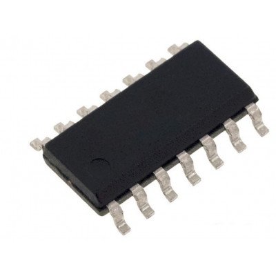
74LS12 IC – (SMD Package) Triple 3-Input Positive NAND Gate IC (7412 IC)
The 74LS12 Triple 3-Input Positive NAND Gates With Collector Outputs contains three 3 input independent gates each of which performs the positive logic NAND function. 74LS12 IC can be soldered directly to the circuit board or can be mounted on a 14 pin IC base. 74LS12 Triple 3-Input Positive NAND Gates With Collector Outputs circuit is designed such that the operation produced on the inputs of pin are (1 & 2 & 3 & 4 NAND 10 & 11 & 12 & 13) is produced on the pin 8 . Operating supply voltages to the IC can vary between 4.5V to 5V and to a maximum of 5.5V and the input logic levels to the device in ?0? (LOW) state is max. 0.7V and for ?1? (HIGH) state is min 2V.
 Boards & Modules
 ARM Microcontroller
 AVR Microcontroller Board
 Arduino boards
 Advance Development Boards
 8051 Development Board
 Audio Amplifier Module
 Current & Volatage Sensor
 Breakout Board
 Flame Sensors
 Force Sensor
 Gas Sensors
 Hall Effect Sensor
 Humidity & Temperature Sensor
 LED Module
 PIR Sensor
 Pressure Sensors
 Proximity Sensor
 Relay Module
 Real Time Clock (RTC) Module
 Touch Sensor
 Ultrasonic Sensor
 Water Level & Water Flow Sensor
 Weighing Scale Sensor


 Ai Thinker ESp Wifi Module
 Pic Devlopment Board & programmer
 Led lights & Strips
 PCBs & Breadboard
 Potentiometer
 Power Transistors
 Resistor & Smd & inductor
 Switches
 Aluminium Heat Sink
 Buzzer & Speaker
 capacitor
 Crystal Oscillators
 Doides
 Electric Fuses
 ICs & Dips
 Power supply module
 Transformer
 Relay Module
 Kits
Kits Magnet
 RF Connectors
 PCT and DC Connectors
 Wires & Heat Shrink
 FFC, FPC, Berg connectors
 Nextion
 Segment
 Seedstudio
 Waveshare
 E Bike Batteries
 E bike Battery Case
 E bike Connectors
 E bike Display
 E bike Kit
 E bike Motors & Controllers
 Electronics Accessories
 Mechanical Accessories
 Display
 Cameras