

CD4015 consists of two identical, independent, 4-stage serial-input/parallel-output registers. Each register has independent CLOCK and RESET inputs as well as a single serial DATA input. “Q” outputs are available from each of the four stages on both registers. All register stages are D-type, master-slave flip-flops. The logic level present at the DATA input is transferred into the first register stage and shifted over one stage at each positive-going clock transition. Resetting of all stages is accomplished by a high level on the reset line. Register expansion to 8 stages using one CD4015 package, or to more than 8 stages using additional CD4015?s is possible.
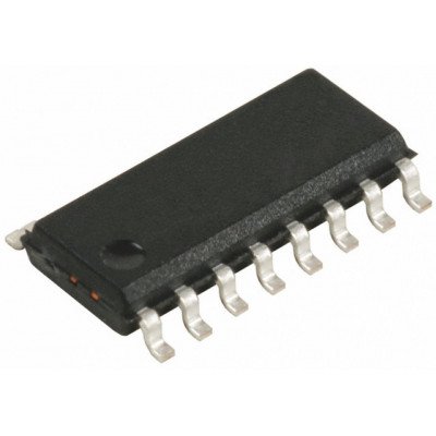
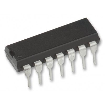
The CD4015-series types are supplied in 16-lead hermetic dual-in-line ceramic packages (F3A suffix), 16-lead dual-in-line plastic package (E suffix), 16-lead small-outline packages (M, M96, MT, and NSR suffixes), and 16-lead thin shrink small-outline packages (PW and PWR suffixes).
Features:-
- Medium speed operation…12 MHz (typ.) clock rate at VDD ? VSS = 10 V
- Fully static operation
- 8 master-slave flip-flops plus input and output buffering
- 100% tested for quiescent current at 20 V
- 5-V, 10-V, and 15-V parametric ratings
- Standardized, symmetrical output characteristics
- Maximum input current of 1 ?A at 18 V over full package-temperature range; 100 nA at 18 V and 25?C
- Noise margin (full package-temperature range) =
- 1 V at VDD = 5 V
- 2 V at VDD = 10 V
- 2.5 V at VDD = 15 V
- Meets all requirements of JEDEC Tentative Standard No. 13B, “Standard Specifications for Description of ?B? Series CMOS Devices”
- Applications:
- Serial-input/parallel-output data queueing
- Serial to parallel data conversion
- General-purpose register
Specifications:-
| Parameter | Specification |
| Part number | CD4015B |
| Technology Family | CD4000 |
| VCC (Min) (V) | 3 |
| VCC (Max) (V) | 18 |
| Voltage (Nom) (V) | 10 |
| F @ nom voltage (Max) (MHz) | 8 |
| ICC @ nom voltage (Max) (mA) | 0.3 |
| tpd @ nom Voltage (Max (ns) | 160 |
| IOL (Max) (mA) | 1.5 |
| IOH (Max) (mA) | -1.5 |
| 3-state output | No |
| Rating | See Data Sheet |
| Operating temperature range (C) | -55 to 125 |
Related Document:-


 Boards & Modules
 ARM Microcontroller
 AVR Microcontroller Board
 Arduino boards
 Advance Development Boards
 8051 Development Board
 Audio Amplifier Module
 Current & Volatage Sensor
 Breakout Board
 Flame Sensors
 Force Sensor
 Gas Sensors
 Hall Effect Sensor
 Humidity & Temperature Sensor
 LED Module
 PIR Sensor
 Pressure Sensors
 Proximity Sensor
 Relay Module
 Real Time Clock (RTC) Module
 Touch Sensor
 Ultrasonic Sensor
 Water Level & Water Flow Sensor
 Weighing Scale Sensor


 Ai Thinker ESp Wifi Module
 Pic Devlopment Board & programmer
 Led lights & Strips
 PCBs & Breadboard
 Potentiometer
 Power Transistors
 Resistor & Smd & inductor
 Switches
 Aluminium Heat Sink
 Buzzer & Speaker
 capacitor
 Crystal Oscillators
 Doides
 Electric Fuses
 ICs & Dips
 Power supply module
 Transformer
 Relay Module
 Kits
Kits Magnet
 RF Connectors
 PCT and DC Connectors
 Wires & Heat Shrink
 FFC, FPC, Berg connectors
 Nextion
 Segment
 Seedstudio
 Waveshare
 E Bike Batteries
 E bike Battery Case
 E bike Connectors
 E bike Display
 E bike Kit
 E bike Motors & Controllers
 Electronics Accessories
 Mechanical Accessories
 Display
 Cameras
Reviews
There are no reviews yet.