

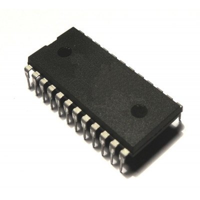

The CD4066 device is a quad bilateral switch intended for the transmission or multiplexing of analog or digital signals. It is pin-for-pin compatible with the CD4016 device, but exhibits a much lower on-state resistance. In addition, the on-state resistance is relatively constant over the full signal-input range.
The CD4066 device consists of four bilateral switches, each with independent controls. Both the p and the n devices in a given switch are biased on or off simultaneously by the control signal. The well of the n-channel device on each switch is tied to either the input (when the switch is on) or to VSS (when the switch is off). This configuration eliminates the variation of the switch-transistor threshold voltage with input signal and, thus, keeps the on-state resistance low over the full operating-signal range.
The advantages over single-channel switches include peak input-signal voltage swings equal to the full supply voltage and more constant on-state impedance over the input-signal range. However, for sample-and-hold applications, the CD4016 device is recommended.
Features:-
- 15-V Digital or ?7.5-V Peak-to-Peak Switching
- 125-? Typical On-State Resistance for
15-V Operation - Switch On-State Resistance Matched to Within
5 ? Over 15-V Signal-Input Range - On-State Resistance Flat Over Full
Peak-to-Peak Signal Range - High On or Off Output-Voltage Ratio:
80 dB Typical at fis = 10 kHz, RL = 1 k? - High Degree of Linearity: <0.5% Distortion Typical at fis = 1 kHz, Vis = 5-Vp-p
VDD ? VSS ? 10-V, RL = 10 k? - Extremely Low Off-State Switch Leakage, Resulting in Very Low Offset Current and High Effective Off-State Resistance: 10 pA Typical at VDD ? VSS = 10-V, TA = 25?C
- Extremely High Control Input Impedance
(Control Circuit Isolated From Signal Circuit):
1012 ? Typical - Low Crosstalk Between Switches: ?50 dB Typical at fis = 8 MHz, RL = 1 k?
- Matched Control-Input to Signal-Output Capacitance: Reduces Output Signal Transients
- Frequency Response,
Switch On = 40 MHz Typical - 100% Tested for Quiescent Current at 20-V
- 5-V, 10-V, and 15-V Parametric Ratings
Specifications:-
| Parameter | Specification |
| Part number | CD4066B |
| Configuration | 1:1 SPST |
| Number of channels (#) | 4 |
| Ron (Typ) (Ohms) | 125 |
| Bandwidth (MHz) | 40 |
| Rating | See Data Sheet |
| Operating temperature range (C) | -55 to 125 |
| Package Group | PDIP|14 |
| Input/output continuous current (Max) (mA) | 10 |
| Supply current (Typ) (uA) | 0.01 |
| CON (Typ) (pF) | 8 |
Related Document:-


 Boards & Modules
 ARM Microcontroller
 AVR Microcontroller Board
 Arduino boards
 Advance Development Boards
 8051 Development Board
 Audio Amplifier Module
 Current & Volatage Sensor
 Breakout Board
 Flame Sensors
 Force Sensor
 Gas Sensors
 Hall Effect Sensor
 Humidity & Temperature Sensor
 LED Module
 PIR Sensor
 Pressure Sensors
 Proximity Sensor
 Relay Module
 Real Time Clock (RTC) Module
 Touch Sensor
 Ultrasonic Sensor
 Water Level & Water Flow Sensor
 Weighing Scale Sensor


 Ai Thinker ESp Wifi Module
 Pic Devlopment Board & programmer
 Led lights & Strips
 PCBs & Breadboard
 Potentiometer
 Power Transistors
 Resistor & Smd & inductor
 Switches
 Aluminium Heat Sink
 Buzzer & Speaker
 capacitor
 Crystal Oscillators
 Doides
 Electric Fuses
 ICs & Dips
 Power supply module
 Transformer
 Relay Module
 Kits
Kits Magnet
 RF Connectors
 PCT and DC Connectors
 Wires & Heat Shrink
 FFC, FPC, Berg connectors
 Nextion
 Segment
 Seedstudio
 Waveshare
 E Bike Batteries
 E bike Battery Case
 E bike Connectors
 E bike Display
 E bike Kit
 E bike Motors & Controllers
 Electronics Accessories
 Mechanical Accessories
 Display
 Cameras
Reviews
There are no reviews yet.