
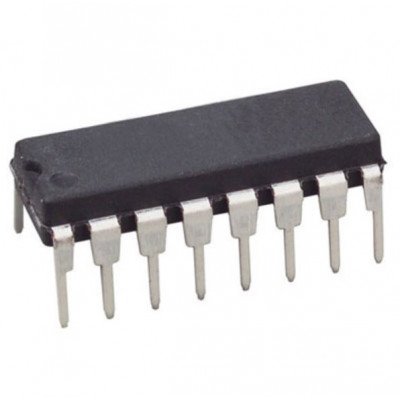


CD4099 8-bit addressable latch is a serial-input, parallel-output storage register that can perform a variety of functions.
Data are inputted to a particular bit in the latch when that bit is addressed (by means of input A0, A1, A2) and when WRITE DISABLE is at a low level. When WRITE DISABLE is high, data entry is inhibited; however, all 8 outputs can be continuously read independent of WRITE DISABLE and address inputs.
A master RESET input is available, which resets all bits to a logic “0” level when RESET and WRITE DISABLE are at a high level. When RESET is at a high level, and WRITE RESET is at a low level, the latch acts as a 1-of-8 demultiplexer; the bit that is addressed has an active output which follows the data input, while all unaddressed bits are held to a logic “0” level.
The CD4099 types are supplied in 16-lead hermetic dual-in-line ceramic packages (F3A suffix), 16-lead dual-in-line plastic package (E suffix), 16-lead small-outline package (M, M96, MT, and NSR suffixes), and 16-lead thin shrink small-outline packages (PW and PWR suffixes).
Features:-
- Serial data input
- Active parallel output
- Storage register capability
- Master clear
- Can function as demultiplexer
- Standardized, symmetrical output characteristics
- 100% tested for quiescent current at 20 V
- Maximum input current of 1 uA at 18 V over full package-temperature range; 100 nA at 18 V and 25?C
- Noise margin (full package-temperature range) =
1 V at VDD = 5 V
2 V at VDD = 10 V
2.5 V at VDD = 15 V - 5-V, 10-V, and 15-V parametric ratings
- Meets all requirements of JEDEC Tentative Standard No. 13B, “Standard Specifications for Description of ?B? Series CMOS Devices”
- Applications:
- Multi-line decoders
- A/D converters
Specifications:-
| Parameter | Specification |
| Part number | CD4099B |
| Technology Family | CD4000 |
| VCC (Min) (V) | 3 |
| VCC (Max) (V) | 18 |
| Bits (#) | 8 |
| Voltage (Nom) (V) | 10 |
| F @ nom voltage (Max) (MHz) | 8 |
| ICC @ nom voltage (Max) (mA) | 0.3 |
| tpd @ nom Voltage (Max) (ns) | 150 |
| IOL (Max) (mA) | 1.5 |
| IOH (Max) (mA) | -1.5 |
| 3-state output | No |
| Operating temperature range (C) | -55 to 125 |
Related Document:-


 Boards & Modules
 ARM Microcontroller
 AVR Microcontroller Board
 Arduino boards
 Advance Development Boards
 8051 Development Board
 Audio Amplifier Module
 Current & Volatage Sensor
 Breakout Board
 Flame Sensors
 Force Sensor
 Gas Sensors
 Hall Effect Sensor
 Humidity & Temperature Sensor
 LED Module
 PIR Sensor
 Pressure Sensors
 Proximity Sensor
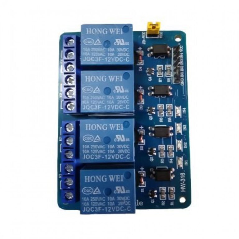
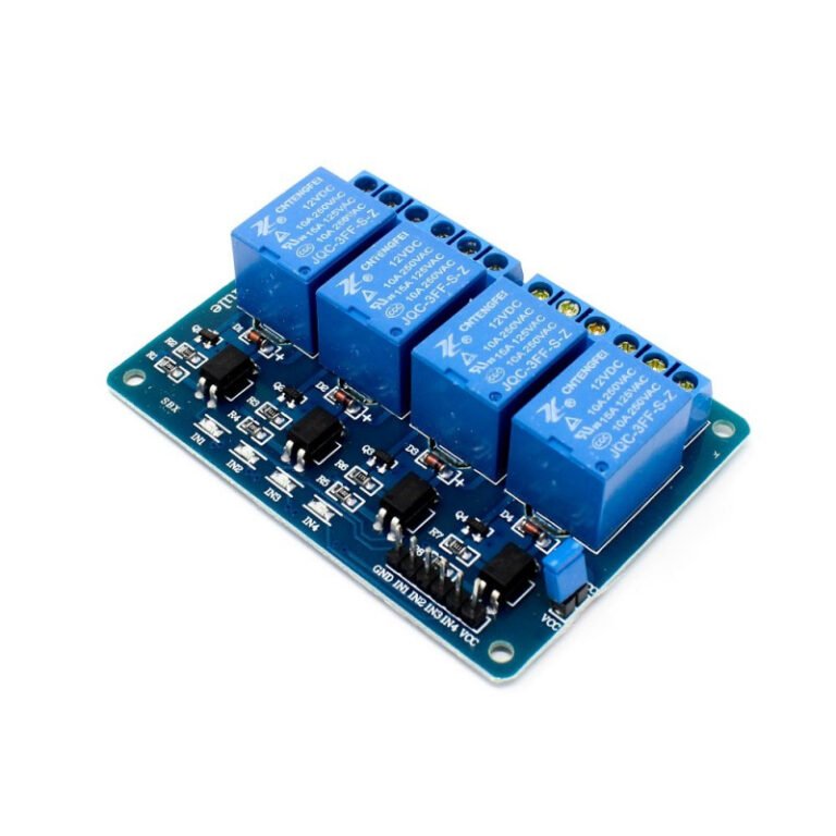
 Relay Module
 Real Time Clock (RTC) Module
 Touch Sensor
 Ultrasonic Sensor
 Water Level & Water Flow Sensor
 Weighing Scale Sensor


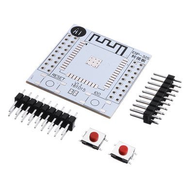
 Ai Thinker ESp Wifi Module
 Pic Devlopment Board & programmer
 Led lights & Strips
 PCBs & Breadboard
 Potentiometer
 Power Transistors
 Resistor & Smd & inductor
 Switches
 Aluminium Heat Sink
 Buzzer & Speaker
 capacitor
 Crystal Oscillators
 Doides
 Electric Fuses
 ICs & Dips
 Power supply module
 Transformer
 Relay Module
 Kits
Kits Magnet
 RF Connectors
 PCT and DC Connectors
 Wires & Heat Shrink
 FFC, FPC, Berg connectors
 Nextion
 Segment
 Seedstudio
 Waveshare
 E Bike Batteries
 E bike Battery Case
 E bike Connectors
 E bike Display
 E bike Kit
 E bike Motors & Controllers
 Electronics Accessories
 Mechanical Accessories
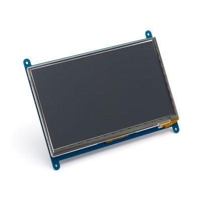
 Display
 Cameras
Reviews
There are no reviews yet.