


74HC93 4-Bit Binary Ripple Counter IC (7493 IC) DIP-14 Package
The 74HC93 are high-speed Si-gate CMOS devices and are pin compatible with low power Schottky TTL (LSTTL). They are specified in compliance with JEDEC standard no. 7A. The 74HC93 are 4-bit binary ripple counters. The devices consist of four master-slave flip-flops internally connected to provide a divide-by-two section and a divide-by-eight section. Each section has a separate clock input (CP0 and CP1) to initiate state changes of the counter on the HIGH-to-LOW clock transition. State changes of the Qn outputs do not occur simultaneously because of internal ripple delays. Therefore, decoded output signals are subject to decoding spikes and should not be used for clocks or strobes.

74HC93 IC – (SMD Package) – 4-Bit Binary Ripple Counter IC (7493 IC)
The 74HC93 are high-speed silicon-gate CMOS devices and are pin-compatible with low power Schottky TTL (LSTTL). These 4-bit binary ripple counters consist of four master-slave flip-flops internally connected to provide a divide-by-two section and a divide- by-eight section. Each section has a separate clock input (CP0 and CP1) to initiate state changes of the counter on the HIGH to LOW clock transition. State changes of the Qn outputs do not occur simultaneously because of internal ripple delays. Therefore, decoded output signals are subject to decoding spikes and should not be used for clocks or strobes. A gated AND asynchronous master reset (MR1 and MR2 is provided which overrides both clocks and resets (clears) all flip-flops. Because the output from the divide by two section is not internally connected to the succeeding stages, the device may be operated in various counting modes. In a 4-bit ripple counter the output Q0 must be connected externally to input CP1. The input count pulses are applied to clock input CP0. Simultaneous frequency divisions of 2, 4, 8, and 16 are performed at the Q0, Q1, Q2, and Q3 outputs as shown in the function table. As a 3-bit ripple counter the input count pulses are applied to input CP1. Simultaneous frequency divisions of 2, 4, and 8 are available at the Q1, Q2, Q3 outputs. Independent use of the first flipflop is available if the reset function coincides with the reset of the 3-bit ripple-through counter.

74LS00 Quad 2 Input NAND Gate IC (7400 IC) DIP-14 Package
The 74LS00 is a 14 Pin Quad 2-Input NAND Gate IC. This device contains four independent gates each of which performs the logic NAND function. NAND gates utilize advanced silicon-gate CMOS technology to achieve operating speeds with the low power consumption of standard CMOS integrated circuits. All gates have buffered outputs.

74LS02 Quad 2-Input NOR Gate IC (7402 IC) DIP-14 Package

74LS03 IC – (SMD Package) Quad 2-input NOR Gate IC (7403 IC)
These devices contain four independent 2-input-NAND gates. The open-collector outputs require pull-up resistors to perform correctly. They may be connected to other open-collector outputs to implement active-low wired-OR or active-high wired-AND functions. Open-collector devices are often used to generate higher VOH levels.

74LS04 Hex Inverter IC (7404 IC) DIP-14 Package
74LS04 is Hex Inverter NOT gate IC. It consists of six inverters which perform logical invert action. output of an inverter is complement of its input logic state i.e. when input is high its output is low and vice versa. device contains six independent gates each of which performs logic INVERT function. Operating voltage is 5V, high-level input voltage is 2V, and low-level input is 0.8V. Contains absolute maximum ratings over operating free-air temperature range, recommended operating conditions, electrical characteristics over recommended operating free-air temperature range.

74LS05 Hex Inverters with Open Collector IC (7405) DIP-14 Package
74LS05 IC – (SMD Package) Hex Inverters with Open-Collector IC (7405 IC)
74LS06 Hex Inverter Buffer IC (7406 IC) DIP-14 Package
This 74LS06 monolithic hex inverter buffers/drivers feature high-voltage open-collector outputs to interface with high-level circuits (such as MOS), or for driving high-current loads, and are also characterized for use as inverter buffers for driving TTL inputs. The ?LS06 has a rated output voltage of 30 V and the ?LS16 has a rated output voltage of 15 V. The maximum sink current for the 74LS06 is 40 mA. The circuits is compatible with most TTL families. Inputs are diode-clamped to minimize transmission-effects, which simplifies design. Typical power dissipation is 175 mW and average propagation delay time is 8 ns. The 74LS06 is characterized for operation from 0?C to 70?C.
74LS06 IC – (SMD Package) – Hex Inverter -Buffer IC (7406 IC)

 Boards & Modules
 ARM Microcontroller
 AVR Microcontroller Board
 Arduino boards
 Advance Development Boards
 8051 Development Board
 Audio Amplifier Module
 Current & Volatage Sensor
 Breakout Board
 Flame Sensors
 Force Sensor
 Gas Sensors
 Hall Effect Sensor
 Humidity & Temperature Sensor
 LED Module
 PIR Sensor
 Pressure Sensors
 Proximity Sensor
 Relay Module
 Real Time Clock (RTC) Module
 Touch Sensor
 Ultrasonic Sensor
 Water Level & Water Flow Sensor
 Weighing Scale Sensor


 Ai Thinker ESp Wifi Module
 Pic Devlopment Board & programmer
 Led lights & Strips
 PCBs & Breadboard
 Potentiometer
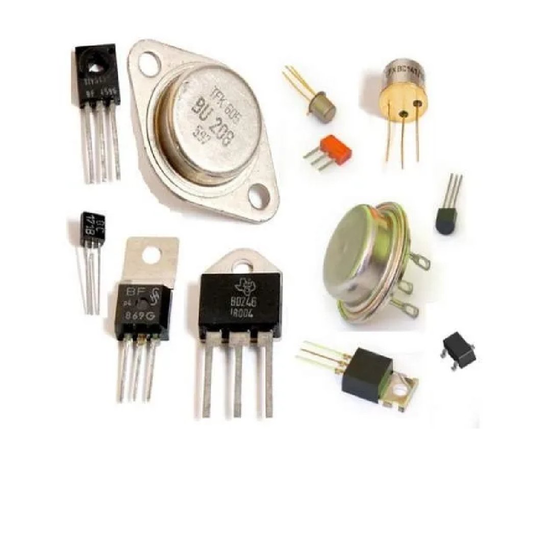
 Power Transistors
 Resistor & Smd & inductor
 Switches
 Aluminium Heat Sink
 Buzzer & Speaker
 capacitor
 Crystal Oscillators
 Doides
 Electric Fuses
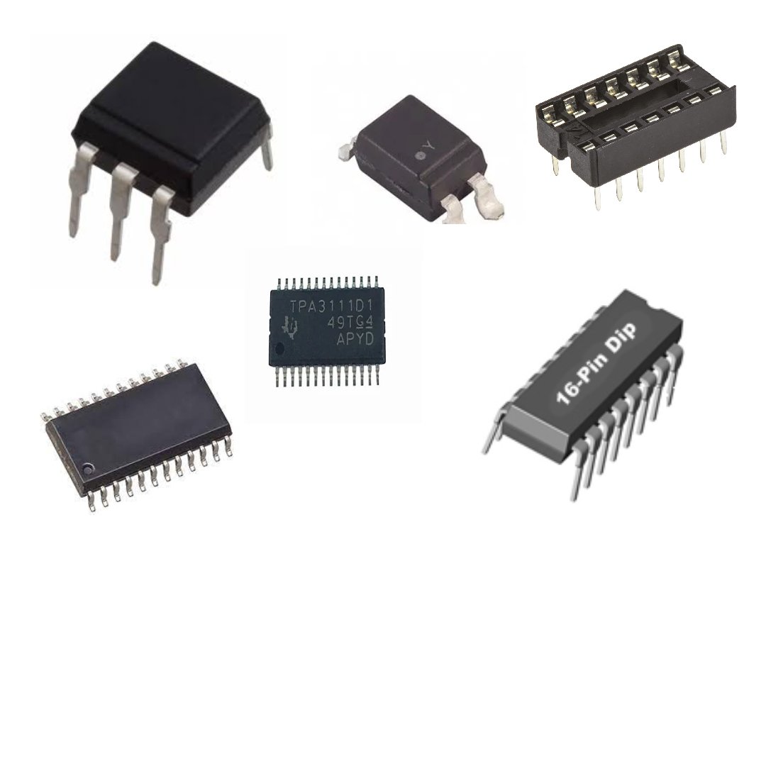
 ICs & Dips
 Power supply module
 Transformer
 Relay Module
 Kits
Kits Magnet
 RF Connectors
 PCT and DC Connectors
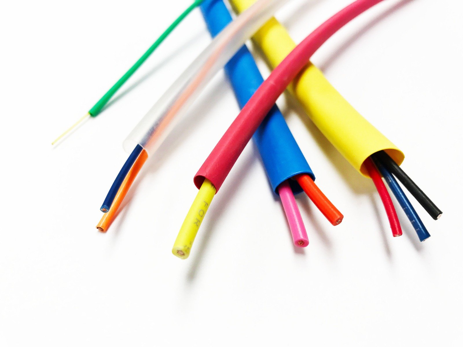
 Wires & Heat Shrink
 FFC, FPC, Berg connectors
 Nextion
 Segment
 Seedstudio
 Waveshare
 E Bike Batteries
 E bike Battery Case
 E bike Connectors
 E bike Display
 E bike Kit
 E bike Motors & Controllers
 Electronics Accessories
 Mechanical Accessories
 Display
 Cameras