


74HC590 IC – (SMD Package) – 8-Bit Binary Counter IC (74590 IC)
The 74HC590 is an 8-bit binary counter with a storage register and 3-state outputs. The storage register has parallel (Q0 to Q7) outputs. The binary counter features master reset counter (MRC) and count enable (CE) inputs. The counter and storage register have separate positive edge triggered clock (CPC and CPR) inputs. If both clocks are connected together, the counter state is always one count ahead of the register. Internal circuitry prevents clocking from the clock enable. A ripple carry output (RCO) is provided for cascading. Cascading is accomplished by connecting RCO of the first stage to CE of the second stage. Cascading for larger count chains can be accomplished by connecting RCO of each stage to the counter clock (CPC) input of the following stage. Inputs include clamp diodes. This enables the use of current limiting resistors to interface inputs to voltages in excess of VCC.
74HC595 8-bit Serial to Parallel Shift Register IC (74595 IC) DIP-16 Package
The 74HC595 high speed shift register utilizes advanced silicon-gate CMOS technology. This device possesses the high noise immunity and low power consumption of standard CMOS integrated circuits, as well as the ability to drive 15 LS-TTL loads. This device contains an 8-bit serial-in, parallel-out shift register that feeds an 8-bit D-type storage register. The storage register has 8 3-STATE outputs. Separate clocks are provided for both the shift register and the storage register.
74HC646 IC – (SMD Package) – Octal Bus Transceiver Register IC (74646 IC)
The M74HC646 are high speed CMOS OCTAL BUS TRANSCEIVERS AND REGISTERS, (3-STATE) fabricated in silicon gate C2 MOS technology. They have the same high speed performance of LSTTL combined with true CMOS low power consumption. These devices consist of bus transceiver circuits with 3-state output, D-type flip-flops, and control circuitry arranged for multiplexed transmission of data directly from the input bus or from the internal registers. Data on the A or B bus will be clocked into the registers on the low-to-high transition of the appropriate clock pin (Clock AB - or Clock BA). Enable(G) and direction (DIR) pins are provided to control the
74HC646 Octal Bus Transceiver Register IC (74646 IC) DIP-24 Package
The M74HC646 are high speed CMOS OCTAL BUS TRANSCEIVERS AND REGISTERS, (3-STATE) fabricated in silicon gate C2 MOS technology. They have the same high speed performance of LSTTL combined with true CMOS low power consumption. These devices consist of bus transceiver circuits with 3-state output, D-type flip-flops, and control circuitry arranged for multiplexed transmission of data directly from the input bus or from the internal registers. Data on the A or B bus will be clocked into the registers on the low-to-high transition of the appropriate clock pin (Clock AB - or Clock BA). Enable(G) and direction (DIR) pins are provided to control the
74HC73 Dual J-K Negative-Edge-Triggered Flip-Flops IC (7473) DIP-14 Package
The 74HC73 is a dual negative edge triggered JK flip-flop with individual J, K, clock (nCP) and reset (nR) inputs and complementary nQ and nQ outputs. The J and K inputs must be stable, one set-up time prior to the HIGH-to-LOW clock transition for predictable operation. (nR) is asynchronous, when LOW it overrides the clock and data inputs, forcing the nQ output LOW and the nQ output HIGH. Schmitt-trigger action in the clock input makes the circuit highly tolerant to slower clock rise and fall times. Inputs include clamp diodes. This enables the use of current limiting resistors to interface inputs to voltages in excess of VCC
74HC73 IC – (SMD Package) – Dual J-K Negative-Edge-Triggered Flip-Flops IC (7473)
The 74HC73 is a high-speed Si-gate CMOS device and is pin compatible with low-power Schottky TTL (LSTTL). The 74HC73 is specified in compliance with JEDEC standard no. 7A. The 74HC is a dual negative-edge triggered JK flip-flop featuring individual J, K, clock (nCP) and reset (nR) inputs; also complementary nQ and nQ outputs. The J and K inputs must be stable one set-up time prior to the HIGH-to-LOW clock transition for predictable operation. The reset (nR) is an asynchronous active LOW input. When LOW, it overrides the clock and data inputs, forcing the nQ output LOW and the nQ output HIGH. Schmitt-trigger action in the clock input makes the circuit highly tolerant to slower clock rise and fall times.

74HC75 4 Bit Bi-Stable Latch IC (7475 IC) DIP-16 Package
74HC75 is 4 Bit Bi-Stable Latch 16 Pin IC. It contains 4 transparent D latches with common enable (gate) on latches 0 and 1 and another common enable on latches 2 and 3. When Q follows D (latch enabled) latch is said to be transparent. Q output will change only on edge of input trigger pulse. small triangle on clock (Cp) input of symbol indicates that device is positive edge-triggered. D and clock inputs are synchronous inputs. set (SD) and reset (RD) inputs are asynchronous. They operate independent of D and Cp. bubbles on set and reset inputs indicate that they are low active. latches are ideally suited for use as temporary storage for binary information between processing units and input output or indicator units.

74HC75 IC – (SMD Package) – 4 Bit Bi-Stable Latch IC (7475 IC)
The 74HC75 is a high-speed Si-gate CMOS device and is pin compatible with low power Schottky TTL (LSTTL). The 74HC75 is specified in compliance with JEDEC standard no. 7A. The 74HC75 has four bistable latches. The two latches are simultaneously controlled by one of two active HIGH enable inputs (LE12 and LE34). When LEnn is HIGH, the data enters the latches and appears at the nQ outputs. The nQ outputs follow the data inputs (nD) as long as LEnn is HIGH (transparent). The data on the nD inputs one set-up time prior to the HIGH-to-LOW transition of the LEnn will be stored in the latches. The latched outputs remain stable as long as the LEnn is LOW.

74HC85 4-bit Magnitude Comparator IC (7485 IC) DIP-16 Package
The 74HC85 are high-speed Si-gate CMOS devices and are pin compatible with low power Schottky TTL (LSTTL). They are specified in compliance with JEDEC standard no. 7A. The 74HC85 are 4-bit magnitude comparators that can be expanded to almost any length. They perform comparison of two 4-bit binary, BCD or other monotonic codes and present the three possible magnitude results at the outputs (QA>B, QA=B and QAB, IA=B and IAB = = LOW and IA=B = HIGH. For words greater than 4-bits, units can be cascaded by connecting outputs QA? and QA=B to the corresponding inputs of the significant comparator.
74HC85 IC – (SMD Package) – 4-bit Magnitude Comparator IC (7485 IC)
The 74HC85 SMD is a 4-bit magnitude comparator that can be expanded to almost any length. They perform comparison of two 4-bit binary, BCD or other monotonic codes and present the three possible magnitude results at the outputs (QA>B, QA=B and QAB, IA=B and IAB = LOW and IA=B = HIGH. For words greater than 4-bits, units can be cascaded by connecting outputs QA>B, QA=B and QA.

74HC86 IC – (SMD Package) – Quad 2-Input EXOR Gate IC (7486 IC)
74HC86 is Quad 2-Input EXOR Gate 14 Pin SMD IC. It is an advanced high speed CMOS 2?input Exclusive?OR gate fabricated with silicon gate CMOS technology. It achieves high speed operation similar to equivalent Bipolar Schottky TTL while maintaining CMOS low power dissipation. Internal circuit is composed of three stages, including a buffer output which provides high noise immunity and stable output. Inputs tolerate voltages up to 7V, allowing interface of 5V systems to 3V systems. Used for Building Arithmetic Logic Circuits, Computational Logic Comparators and Error Detection Circuits and True/Complement Element.
74HC86 Quad 2-Input EXOR Gate IC (7486 IC) DIP-14 Package
74HC86 is Quad 2-Input EXOR Gate 14 Pin IC. It is an advanced high speed CMOS 2?input Exclusive?OR gate fabricated with silicon gate CMOS technology. It achieves high speed operation similar to equivalent Bipolar Schottky TTL while maintaining CMOS low power dissipation. Internal circuit is composed of three stages, including a buffer output which provides high noise immunity and stable output. Inputs tolerate voltages up to 7V, allowing interface of 5V systems to 3V systems. Used for Building Arithmetic Logic Circuits, Computational Logic Comparators and Error Detection Circuits and True/Complement Element.

 Boards & Modules
 ARM Microcontroller
 AVR Microcontroller Board
 Arduino boards
 Advance Development Boards
 8051 Development Board
 Audio Amplifier Module
 Current & Volatage Sensor
 Breakout Board
 Flame Sensors
 Force Sensor
 Gas Sensors
 Hall Effect Sensor
 Humidity & Temperature Sensor
 LED Module
 PIR Sensor
 Pressure Sensors
 Proximity Sensor
 Relay Module
 Real Time Clock (RTC) Module
 Touch Sensor
 Ultrasonic Sensor
 Water Level & Water Flow Sensor
 Weighing Scale Sensor


 Ai Thinker ESp Wifi Module
 Pic Devlopment Board & programmer
 Led lights & Strips
 PCBs & Breadboard
 Potentiometer
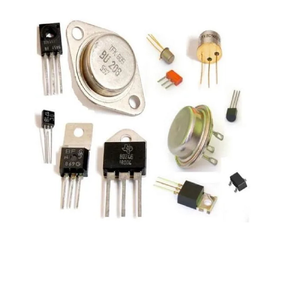
 Power Transistors
 Resistor & Smd & inductor
 Switches
 Aluminium Heat Sink
 Buzzer & Speaker
 capacitor
 Crystal Oscillators
 Doides
 Electric Fuses
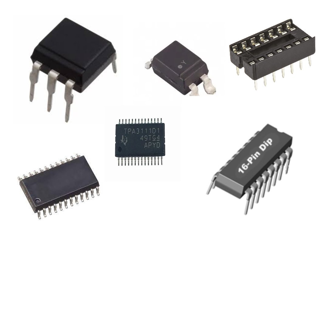
 ICs & Dips
 Power supply module
 Transformer
 Relay Module
 Kits
Kits Magnet
 RF Connectors
 PCT and DC Connectors
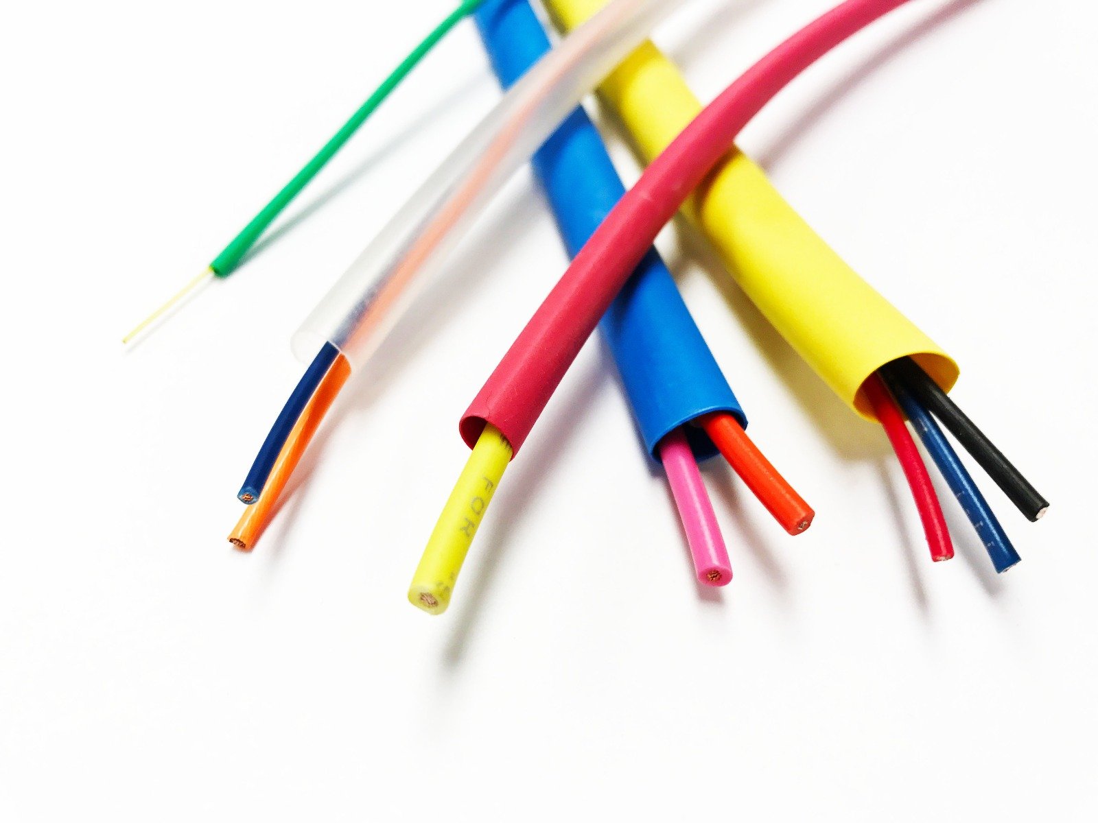
 Wires & Heat Shrink
 FFC, FPC, Berg connectors
 Nextion
 Segment
 Seedstudio
 Waveshare
 E Bike Batteries
 E bike Battery Case
 E bike Connectors
 E bike Display
 E bike Kit
 E bike Motors & Controllers
 Electronics Accessories
 Mechanical Accessories
 Display
 Cameras