


74LS54 IC – (SMD Package) Quad 2-Input AND/OR Inverter Gate IC (7454 IC)

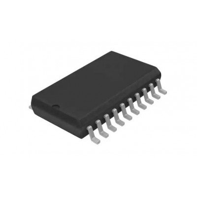
74LS573 3-State Octal D-Type Latch IC (74573) DIP-20 Package

74LS573 IC – (SMD Package) – 3-State Octal D-Type Latch IC (74573 IC)

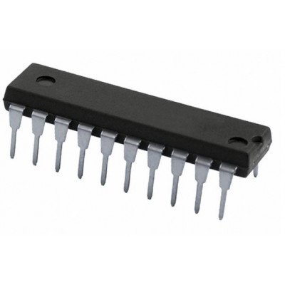
74LS598 8-Bit Shift Register IC (74598) DIP-20 Package
74LS598 IC – (SMD Package) – 8-Bit Shift Register IC (74598 IC)
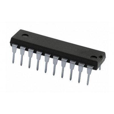
74LS603 Memory Refresh Controllers IC (74603) DIP-20 Package
The LS603A memory refresh controllers contain one 8-bit synchronous counter, nine 3-state buffer drivers, four RC controlled multivibrators, and other control circuitry on a single monolithic chip. These devices are designed to provide RAS-only refresh on 4K, 16K, and 64K dynamic RAMs. The LS600A and LS601A provide transparent refresh while the LS603A provides cycle steal refresh. in addition, a burst-mode timer is provided to warn the CPU that the maximum allowable refresh time is about to be violated.
74LS629 IC – (SMD Package) – Voltage Controlled Oscillators IC (74629 IC)
These voltage-controlled oscillators (VCOs) are Improved versions of the original VCO family: SN54LS124, SN54LS324 thru SN54LS327, SN74LS124, and SN74LS324 thru SN74LS327. These new devices feature improved voltage-to frequency linearity, range, and compensation. With the exception of the "LS624 and LS628, all of these devices feature two independent VCOs in a single monolithic chip. The 'LS624, 'LS625, LS626, and LS628 have complementary Z outputs. The output frequency for each VCO is established by a single external component (either a capacitor or crystal) in combination with voltage-sensitive inputs used for frequency control and frequency range. Each device has a voltage-sensitive input for frequency control; however, the 'LS624, 'LS628, and 'LS629 devices also have one for frequency range. (See Figures 1 thru 6).

74LS629 Voltage Controlled Oscillators IC (74629) DIP-16 Package
These voltage-controlled oscillators (VCOs) are Improved versions of the original VCO family: SN54LS124, SN54LS324 thru SN54LS327, SN74LS124, and SN74LS324 thru SN74LS327. These new devices feature improved voltage-to frequency linearity, range, and compensation. With the exception of the "LS624 and LS628, all of these devices feature two independent VCOs in a single monolithic chip. The 'LS624, 'LS625, LS626, and LS628 have complementary Z outputs. The output frequency for each VCO is established by a single external component (either a capacitor or crystal) in combination with voltage-sensitive inputs used for frequency control and frequency range. Each device has a voltage-sensitive input for frequency control; however, the 'LS624, 'LS628, and 'LS629 devices also have one for frequency range. (See Figures 1 thru 6).
74LS669 IC – (SMD Package) – Synchronous 4-Bit Up/Down Binary Counter IC (74669 IC)
The 74LS669 is a synchronous 4-bit up/down counter. The LS669 is a 4-bit binary counter. For high speed counting applications, this presettable counter features an internal carry lookahead for cascading purposes. By clocking all flip-flops simultaneously so the outputs change coincident with each other (when instructed to do so by the count enable inputs and internal gating) synchronous operation is provided. This helps to eliminate output counting spikes, normally associated with asynchronous (ripple-clock) counters. The four master-slave flip-flops are triggered on the rising (positive-going) edge of the clock waveform by a buffered clock input. Circuitry of the load inputs allows loading with the carry-enable output of the cascaded counters. Because loading is synchronous, disabling of the counter

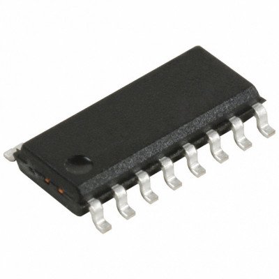
74LS669 Synchronous 4-Bit Up/Down Binary Counter IC (74669) DIP-14 Package
The 74LS669 is a synchronous 4-bit up/down counter. The LS669 is a 4-bit binary counter. For high speed counting applications, this presettable counter features an internal carry lookahead for cascading purposes. By clocking all flip-flops simultaneously so the outputs change coincident with each other (when instructed to do so by the count enable inputs and internal gating) synchronous operation is provided. This helps to eliminate output counting spikes, normally associated with asynchronous (ripple-clock) counters. The four master-slave flip-flops are triggered on the rising (positive-going) edge of the clock waveform by a buffered clock input. Circuitry of the load inputs allows loading with the carry-enable output of the cascaded counters. Because loading is synchronous, disabling of the counter

74LS670 4-By-4 Register Files With 3-State Outputs IC (74670 IC) DIP-16 Package
The SN54L5670 and SN74LS670 MS1 16-bit TTL register film incorporate the equivalent of 98 gates. The register file is organized as 4 words of 4 bits each and separate on-chip decoding is provided for addressing the four word locations to either write-in or retrieve data. This permits simultaneous writing into one location and reading from another word location. Four data inputs are available which are used to supply the 4-bit word to be stored. Location of the word is determined by the write-address inputs A and B in conjunction with a write-enable signal. Data applied at the inputs should be in its true form That is, if a high-level signal is desired from the output, a high-level is applied at the data input for that particular bit location. The latch inputs are arranged so that new data will be accepted only if both internal address gate inputs are high. When this condition exists, data at the D input is transferred to the latch output. When the write-enable input, Ow, is high, the data in puts are inhibited and their levels can cause no change in the information stored in the internal latches. When the read-enable Input, Gn, is high, the data outputs are inhibited and go into the high-impedance stats

 Boards & Modules
 ARM Microcontroller
 AVR Microcontroller Board
 Arduino boards
 Advance Development Boards
 8051 Development Board
 Audio Amplifier Module
 Current & Volatage Sensor
 Breakout Board
 Flame Sensors
 Force Sensor
 Gas Sensors
 Hall Effect Sensor
 Humidity & Temperature Sensor
 LED Module
 PIR Sensor
 Pressure Sensors
 Proximity Sensor
 Relay Module
 Real Time Clock (RTC) Module
 Touch Sensor
 Ultrasonic Sensor
 Water Level & Water Flow Sensor
 Weighing Scale Sensor


 Ai Thinker ESp Wifi Module
 Pic Devlopment Board & programmer
 Led lights & Strips
 PCBs & Breadboard
 Potentiometer
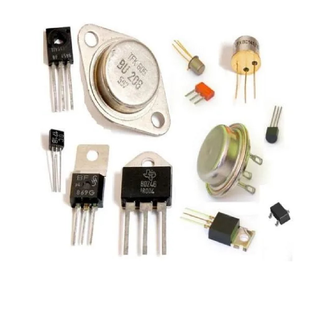
 Power Transistors
 Resistor & Smd & inductor
 Switches
 Aluminium Heat Sink
 Buzzer & Speaker
 capacitor
 Crystal Oscillators
 Doides
 Electric Fuses
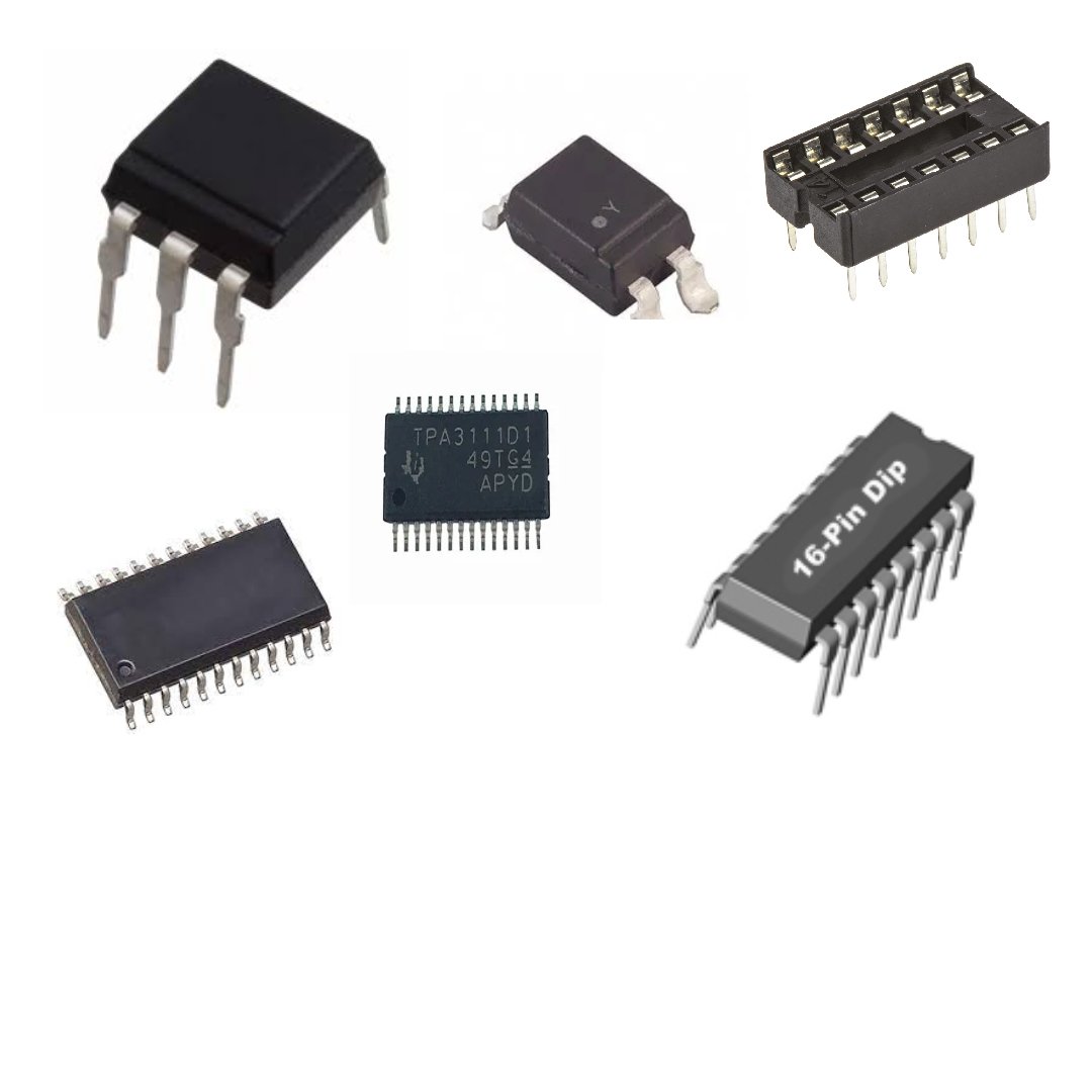
 ICs & Dips
 Power supply module
 Transformer
 Relay Module
 Kits
Kits Magnet
 RF Connectors
 PCT and DC Connectors
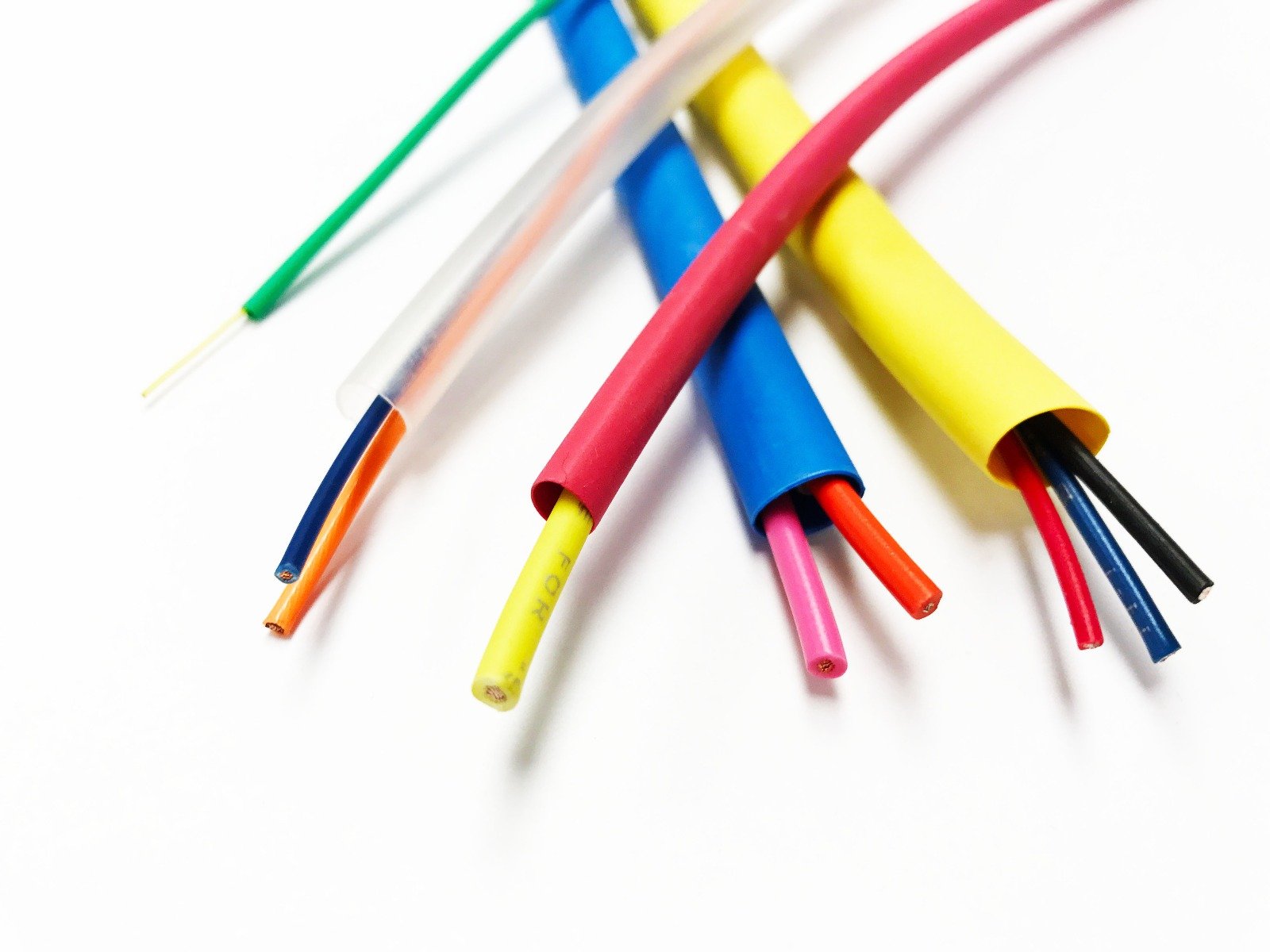
 Wires & Heat Shrink
 FFC, FPC, Berg connectors
 Nextion
 Segment
 Seedstudio
 Waveshare
 E Bike Batteries
 E bike Battery Case
 E bike Connectors
 E bike Display
 E bike Kit
 E bike Motors & Controllers
 Electronics Accessories
 Mechanical Accessories
 Display
 Cameras