


74HC04 IC – (SMD Package) – Hex Inverter IC (7404 IC)

74HC08 IC – (SMD Package) – Quad 2-Input AND Gate IC (7408 IC)
74HC08 Quad 2-Input AND Gate IC (7408 IC) DIP-14 Package
74HC109 Dual J-K Negative-Edge-Triggered Flip-Flops IC (74109) DIP-16 Package
74HC109 Dual J-K Positive-Edge-Triggered Flip-Flop IC ? DIP-16 Package The 74HC109 is a dual positive edge triggered JK flip-flop featuring individual nJ and nK inputs. It has clock (nCP) inputs, set (nSD) and reset (nRD) inputs and complementary nQ and nQ outputs. The set and reset are asynchronous active LOW inputs and operate independently of the clock input. The nJ and nK inputs control the state changes of the flip-flops as described in the mode select function table. The nJ and nK inputs must be stable one set-up time prior to the LOW-to-HIGH clock transition for predictable operation. The JK design allows operation as a D-type flip-flop by connecting the nJ and nK inputs together. Inputs include clamp diodes. It enables the use of current limiting resistors to interface inputs to voltages in excess of VCC.

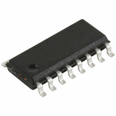
74HC109 IC – (SMD Package) – Dual J-K Positive-Edge-Triggered Flip-Flops IC (74109 IC)
The 74HC109 is a dual positive edge triggered JK flip-flop featuring individual nJ and nK inputs. It has clock (nCP) inputs, set (nSD) and reset (nRD) inputs and complementary nQ and nQ outputs. The set and reset are asynchronous active LOW inputs and operate independently of the clock input. The nJ and nK inputs control the state changes of the flip-flops as described in the mode select function table. The nJ and nK inputs must be stable one set-up time prior to the LOW-to-HIGH clock transition for predictable operation. The JK design allows operation as a D-type flip-flop by connecting the nJ and nK inputs together. Inputs include clamp diodes. It enables the use of current limiting resistors to interface inputs to voltages in excess of VCC. Schmitt-trigger action in the clock input makes the circuit highly tolerant to slower clock rise and fall times.
74HC123 IC – (SMD Package) – Dual Retriggerable Monostable Multivibrator IC (74123)
74HC123 IC – (SMD Package) – Dual Retriggerable Monostable Multivibrator IC (74123)

74HC137 3-to-8 line Decoder/Demultiplexer IC (74138 IC) DIP-16 Package

74HC137 IC – (SMD Package) – 3-to-8 line Decoder/Demultiplexer IC (74138 IC)
74HC137 IC – (SMD Package) – 3-to-8 line Decoder/Demultiplexer IC (74138 IC)
74HC138 3-to-8 line Decoder/Demultiplexer IC (74138 IC) DIP-16 Package
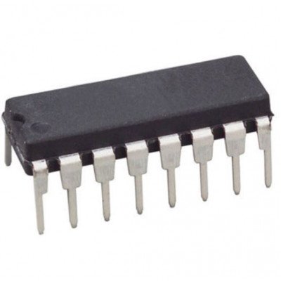
The 74HC138 decoder utilizes advanced silicon-gate CMOS technology and is well suited to memory address decoding or data routing applications. The circuit features high noise immunity and low power consumption usually associated with CMOS circuitry, yet has speeds comparable to low power Schottky TTL logic. The 74HC138 has 3 binary select inputs (A, B, and C). If the device is enabled, these inputs determine which one of the eight normally HIGH outputs will go LOW. Two active LOW and one active HIGH enables (G1, G2A and G2B) are provided to ease the cascading of decoders. The decoder?s outputs can drive 10 low power Schottky TTL equivalent loads, and are functionally and pin equivalent to the 74LS138. All inputs are protected from damage due to static discharge by diodes to VCC and ground.
74HC138 IC – (SMD Package) – 3-to-8 line Decoder/Demultiplexer IC (74138 IC)
The 74HC138 decoder utilizes advanced silicon-gate CMOS technology and is well suited to memory address decoding or data routing applications. The circuit features high noise immunity and low power consumption usually associated with CMOS circuitry, yet has speeds comparable to low power Schottky TTL logic. The 74HC138 has 3 binary select inputs (A, B, and C). If the device is enabled, these inputs determine which one of the eight normally HIGH outputs will go LOW. Two active LOW and one active HIGH enables (G1, G2A and G2B) are provided to ease the cascading of decoders. The decoder?s outputs can drive 10 low power Schottky TTL equivalent loads, and are functionally and pin equivalent to the 74LS138. All inputs are protected from damage due to static discharge by diodes to VCC and ground.
 Boards & Modules
 ARM Microcontroller
 AVR Microcontroller Board
 Arduino boards
 Advance Development Boards
 8051 Development Board
 Audio Amplifier Module
 Current & Volatage Sensor
 Breakout Board
 Flame Sensors
 Force Sensor
 Gas Sensors
 Hall Effect Sensor
 Humidity & Temperature Sensor
 LED Module
 PIR Sensor
 Pressure Sensors
 Proximity Sensor
 Relay Module
 Real Time Clock (RTC) Module
 Touch Sensor
 Ultrasonic Sensor
 Water Level & Water Flow Sensor
 Weighing Scale Sensor


 Ai Thinker ESp Wifi Module
 Pic Devlopment Board & programmer
 Led lights & Strips
 PCBs & Breadboard
 Potentiometer
 Power Transistors
 Resistor & Smd & inductor
 Switches
 Aluminium Heat Sink
 Buzzer & Speaker
 capacitor
 Crystal Oscillators
 Doides
 Electric Fuses
 ICs & Dips
 Power supply module
 Transformer
 Relay Module
 Kits
Kits Magnet
 RF Connectors
 PCT and DC Connectors
 Wires & Heat Shrink
 FFC, FPC, Berg connectors
 Nextion
 Segment
 Seedstudio
 Waveshare
 E Bike Batteries
 E bike Battery Case
 E bike Connectors
 E bike Display
 E bike Kit
 E bike Motors & Controllers
 Electronics Accessories
 Mechanical Accessories
 Display
 Cameras